Technical Brief
Creating SI- and PI-Aware High-Speed Memory Interfaces
Overview
Introduction
DDR5 is a major signal integrity (SI) and power integrity (PI) challenge. This includes the IC package and where it is placed on a board. Key contributing factors are increasing IC speeds and data transmission rates combined with decreases in power-supply voltages, and denser, smaller geometries. Stacked die and packages, higher pin counts, and greater electrical performance constraints add to the challenge. Savvy SI experts who successfully implement memory interfaces, such as DDR4 and DDR5, face major challenges such as an increase in data-rate-to-gigabit speeds and tight timing budgets.
System-Level Analysis
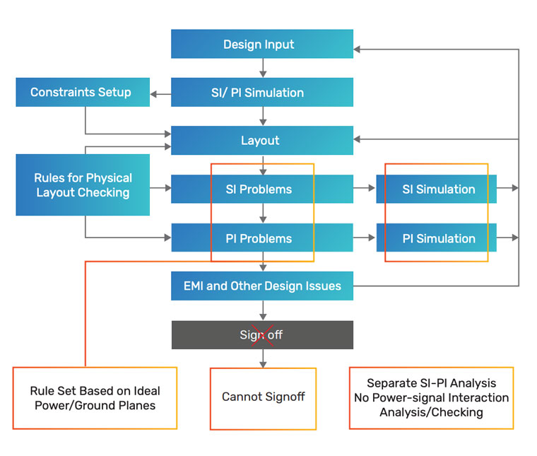
The typical design workflow assumes an ideal power distribution network (PDN) without considering the undesired effects of coupled signal, power, and ground planes that invariably impact PCB SI. When analyzing PI and SI issues separately, power-based SI issues such as simultaneous switching noise (SSN) can also crop up, causing failures (Figure 1).
In-Design Simulation and Analysis
Power Integration
Accurate system-level analysis of PI requires AC and DC power analysis of IC packages with signoff-level accuracy and PI solutions that seamlessly interface with IC packaging and physical design solutions.
Power-Aware Signal Integrity
While the typical design workflow assumes an ideal PDN, power-aware SI (Figure 2) not only considers non-ideal data signals, but also the non-ideal PDN. For example, noise in the PDN primarily affects the system jitter performance, further adding up to the timing constraint of DDR interfaces.
Typically, the power and ground planes are identical for computing characteristic impedance in a 2D simulation. Plane bouncing, or the variation of the potential difference between the power and ground nodes across the surface of the planes, couples with the reflections from a trace impedance mismatch. Any coupling between the power/ ground plane and data traces leads to crosstalk. Eventually, crosstalk and reflections cause delay changes, and thus affect the timing, as it is a measure of the undesired movement of energy from one trace to another.
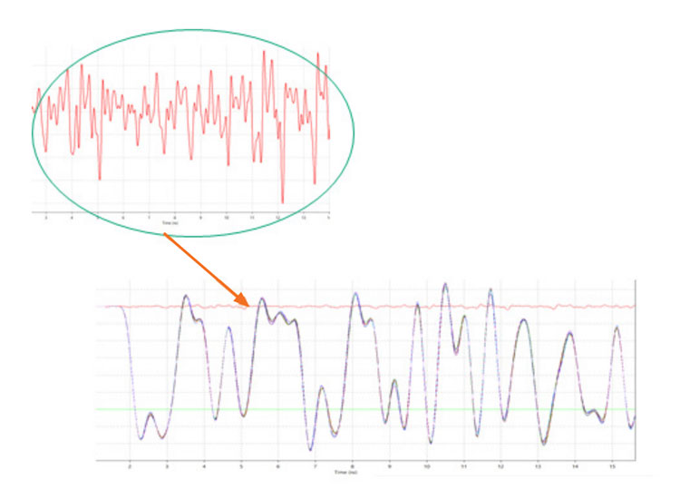
Simultaneous switching signals on the DDR4/DDR5 data bus with a non-ideal current return path can cause SSN. Each bit in the parallel data lines can act independently of one another, potentially creating instances of greater load on the power rails when the signals toggle simultaneously. This simultaneous switching can cause a drop in rail voltage, which, in turn, raises the ground voltage to a non-zero value within the device. Ultimately, SSN adversely affects the analysis of random jitter in eye diagrams as well as generating additional constraints in optimizing the system noise margin for DDR memory.
Typically, SSN analysis can be performed only by an analysis tool utilizing both special I/O (power-aware IBIS 5.0+) models and interconnect models (coupled signal, power, and ground). While the IBIS 5.0+ models can be extrapolated from the memory controller and memory provider, the power-aware interconnect models are extracted from a completed design. Classic SI tools are not equipped with the right field solvers to adequately complete the task of SSN analysis. Moreover, once a design is completely laid out and routed, it is difficult to turn back and optimize while meeting deadlines.
Power-Aware DRCs
Traditional design rule checks (DRCs) for most commercial simulation platforms do not account for noise effects on the signals, with only a geometrical rule check. This makes it difficult to detect any “power-aware” violation of design constraints or to fine-tune SI/PI issues during the in-design and post-layout analysis.
While many engineers would like to use a full-wave 3D tool for interconnect extraction, power-aware analysis typically uses S-parameters created with a hybrid solver. Engineers often resort to hybrid solvers that utilize a field solution, circuit equivalent model, or both. With time-domain SPICE-like simulators, you can extract a simple lumped-element (RLC) Cadence Sigrity Broadband SPICE model from the frequency responses obtained via simulation, which results in a simplified mathematical representation of the passive I/O system behavior.
When the speed in obtaining simulation results is cut down drastically from a full-wave 3D approach, it often leads to less accurate modeling at higher frequencies, particularly for the multigigabit channels with complicated structures found in DDR interfaces such as serpentine line, transitions, and back-drill. Moreover, extracting time-domain simulations from the large interconnect models can cause convergence issues as S-parameter models do not have information at DC and may not behave at lower frequencies.
The “cut and stitch” approach offers an alternative to the lengthy 3D full-wave and less accurate hybrid solvers by dividing areas of interest into partitions where an engineer can select any solver of choice to accurately model a section of PCB. This way, the portions of the PCB that require more complex analysis can be modeled in 3D full-wave while saving hours of time for modeling less desired sections with hybrid tools. However, while this does save time on model generation, an engineer still will have to extract a SPICE model every time corrective adjustments are made in layout in order to understand the power-based SI variations.
The FDTD Approach
One of the methods used for analyzing time-varying interactions between data and power/ground planes, is the use of S-parameter extraction, which comes with potential convergence issues. A better approach would be to employ a finite-difference time-domain (FDTD) technology together with a hybrid solver by integrating a circuit solver, transmission line solver, and a fast electromagnetic (EM) field solver to analyze time-varying interactions between data and power/ground planes, as shown in Figure 3. Linear excitations are given to a large number of signal nets to report signal quality with coupling noise. This eliminates the need for large S-parameter files and nonlinear analysis without compromising on data accuracy.
Augmenting this typical design workflow at extraction with a hybrid solver utilizing the FDTD method can allow an engineer to rapidly analyze and assess any power-aware SI issues without the need to repeatedly perform model extraction. This ultimately yields more accurate simulation results at the PCB/IC package level with both accuracy and speed for an overall quicker time to market.
A noteworthy benefit of this can readily be seen in a DDR interface, for instance, where the high routing density already creates complex layout problems in length matching, spacing, and data signal grouping while meeting crosstalk, timing, cost, and space constraints. Sticking with conservative line lengths and space may fulfill crosstalk and timing specifications but will create a bigger board.
In addition, traditional SPICE time-domain simulations typically have more pronounced non-passive and non-casual issues due to the large number of DDR signals, DDR power/ground nets, and decoupling capacitors (decaps) included in the simulation. Implementing an FDTD method with a hybrid solver can allow for more accurate simulation results that match the lab results with a quicker time to market, adding the ultimate level of signoff using 3D models for the full DDR bus interface.
The Sigrity solution provides high-speed system designers with the most comprehensive, end-to-end, in-design interconnect modeling and SI and PI simulation for PCB and IC packages. It also helps address power-aware SI and power ripple due to signal switching.
Signoff with 3D Full-Wave Modeling
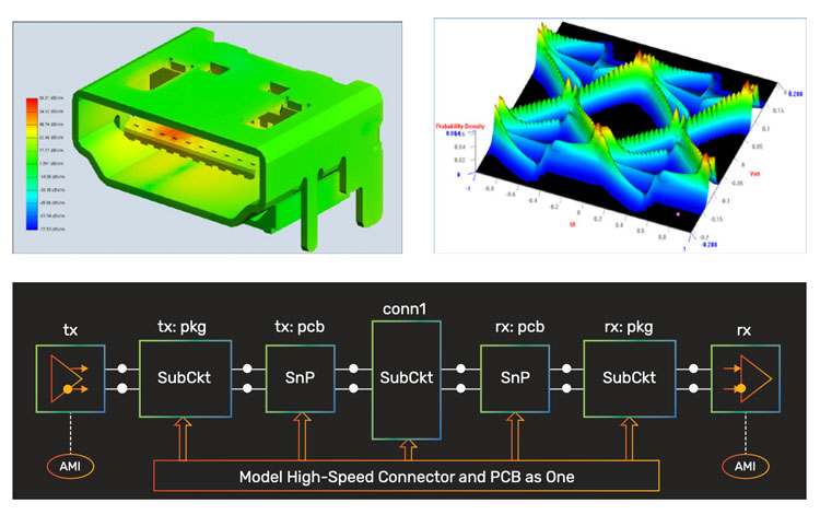
For final signoff, accuracy is paramount. For accuracy, memory buses need to be extracted in their entirety with power and ground. This usually is too large a job for most 3D full-wave modeling tools and causes convergence and stability issues; advanced multi-chip DDR interfaces can involve the simulation of hundreds of ports.
In the finite element method, convergence is typically reached by perturbing a solution into smaller time steps to produce smoother output curves against a tradeoff of the simulation time. As simulation progresses with every step, stability relates to the decay in error. A solution needs to exhibit both stability and convergence in order to reach an agreement between the solution of the partial differential equations and the computed solution found with the discretization process.
Due to the lack of computational resources to adequately simulate a large DDR interface, designers who choose to use 3D full-wave extractions quite often segment their design into smaller pieces. This requires a high level of expertise and can be prone to errors. Moreover, this method also does not typically lend itself to an iterative design process—if changes are made in the layout, model extraction must be performed before rerunning the simulation.
That is changing with the availability of Cadence’s Clarity 3D Solver, a key component in the Intelligent System Design methodology required by advanced electronic product design teams. The Clarity 3D Solver delivers faster simulation performance and unbounded capacity compared to legacy field solver technology (Figure 4). It’s optimized to distribute a job across multiple low-cost computers while remaining equally efficient when running on a more powerful and expensive server with terabytes of memory. This allows Clarity 3D Solver to create highly accurate S-parameter models for use in SI and PI analyses. Furthermore, Clarity 3D Solver eliminates the risk of manually reducing the size of structures being modeled.
Conclusion
High-speed memory interfaces involve the most challenging SI problems that experts face today, with an increase in data-rate-to-gigabit speeds and a tight timing budget. The multi-gigabit parallel bus interfaces involve declining voltage swings, equalized transceivers, tight bit-error-rate (BER) targets, and matched transmission line lengths. Understanding the effects of a non-ideal PDN on SI is no longer optional in order to meet the tight timing constraints. Using the traditional SI analysis workflow can often be a cumbersome process as power-aware SI analysis is often done post-layout, where every change in layout requires repeated model extractions in order to adequately understand the SI effects from fluctuations in power and ground rails.
A proven end-to-end in-design flow, such as that provided by Cadence’s Sigrity technologies together with the signoff solution, Clarity 3D Solver, will minimize design iterations and help improve design margins, getting products to market on time and on budget.