Technical Brief
RF to mmWave Design for Systems
Empowered by AWR Design Environment V16
Overview
Introduction
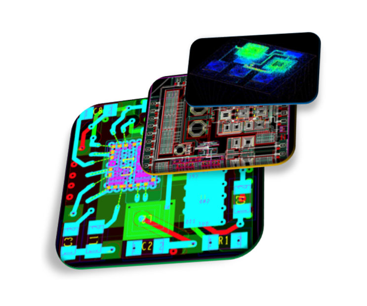
RF-enabled next-generation communication systems and connected devices are differentiated by their performance, size, and cost. Traditionally, custom proprietary IC designs, leveraging the latest advanced-node technology, were developed to meet these product requirements. Increasingly these challenges are being met by moving beyond single IC solutions. Today’s electronic systems often integrate heterogeneous technologies (Figure 1) to mitigate the high cost of homogeneous system-on-chip (SoC) solutions by enabling designers to combine proven RFIC and monolithic microwave IC (MMIC) designs on substrates using newer packaging and integration technologies.
Engineers trying to bring these products to market need best-in-class simulation technology and design automation to accurately predict the performance of larger, densely integrated circuits and subsystems designed for broadband and millimeter-wave (mmWave) spectrum. In addition, since these products are developed by diverse engineering teams across multiple design tools, RF design software must provide interoperability with the broader class of EDA tools used in the development of mixed-signal electronic systems.
The latest release, version 16 (V16), of the Cadence AWR Design Environment platform, including Microwave Office software. Visual System Simulator (VSS) communications and radar systems design software, and AXIEM 3D planar electromagnetic (EM) and Analyst 3D FEM simulators, introduces groundbreaking cross-platform interoperability to support RF IP integration for heterogeneous technology development across Cadence Virtuoso, Allegro PCB, Spectre simulation, and IC package design platforms, delivering up to a 50% reduction in turnaround time compared to competing workflows. The V16 release further introduces seamless integration with Clarity 3D Solver and Celsius Thermal Solver, delivering unconstrained capacity for electrothermal performance analysis of large-scale and complex RF systems.
With AWR Design Environment V16, Cadence addresses RF/ microwave design and integration through the company’s Intelligent System Design strategy, which delivers computational software capabilities across all design elements of electronic systems. At the core of this strategy is design excellence, including an optimized EDA portfolio of tools with best-in-class RF, microwave, and mmWave circuit, system, and EM analysis, IP for semiconductor, package, and PCB design, and scalable access in the cloud.
The V16 Advantage
Advanced integration methodologies result in smaller and more efficient systems. However, these highly integrated systems are more complicated and prone to error due to the interdependencies of the individual components, the complex network of cross-fabric interconnects, and the challenges of assembling cross-platform design data from multiple sources. To address these design obstacles, AWR Design Environment V16 provides an enhanced platform for developing MMIC and RF PCB IP (Figure 2). Design teams can incorporate their MMIC and RF PCB IP into electronic systems composed of ICs and interposers, PCBs, and modules from a wide array of process technologies through proven capabilities in Cadence’s EDA software portfolio, including Allegro PCB Designer for PCBs and SiPs, and the Virtuoso platform for RFICs and modules.
-
 Powerful - Turn concepts into real RF/microwave components, optimized for performance and ready for easy integration into multi-fabric systems that are right the first time
 - Insightful - Capture true RF system performance with tightly coupled EM and thermal analysis for solving large, complex structures and heat-generating RF power applications
- Connected - Embeddable and re-usable Microwave Office software ushers in a new era of unprecedented cross-platform workflows to Allegro and Virtuoso platforms for chip, package, board, and module design
Highlights
Platform Interoperability
Leveraging shared architecture/data across Cadence EDA solutions, the V16 release provides for new RF workflows that take completed IP design from Microwave Office software and pass both the schematic and layout designs to the Virtuoso and/or Allegro platforms as data in a unified library that contains all the building blocks of the circuit design. This enables design teams to operate the Allegro SiP or Virtuoso SiP bi-directional implementation flow and Virtuoso RF Solution physical implementation flow as the primary layout tool, with the AWR Design Environment software providing the RF IP schematic/layout design data. The Virtuoso RF Solution flow captures Microwave Office RF IP, allowing designers to represent, integrate, and verify the MMIC and embedded RF package design within a single environment. The shared database enables more practical package and IC co-design by simplifying the design flow with easy and reliable access to RF IP developed within Microwave Office software.
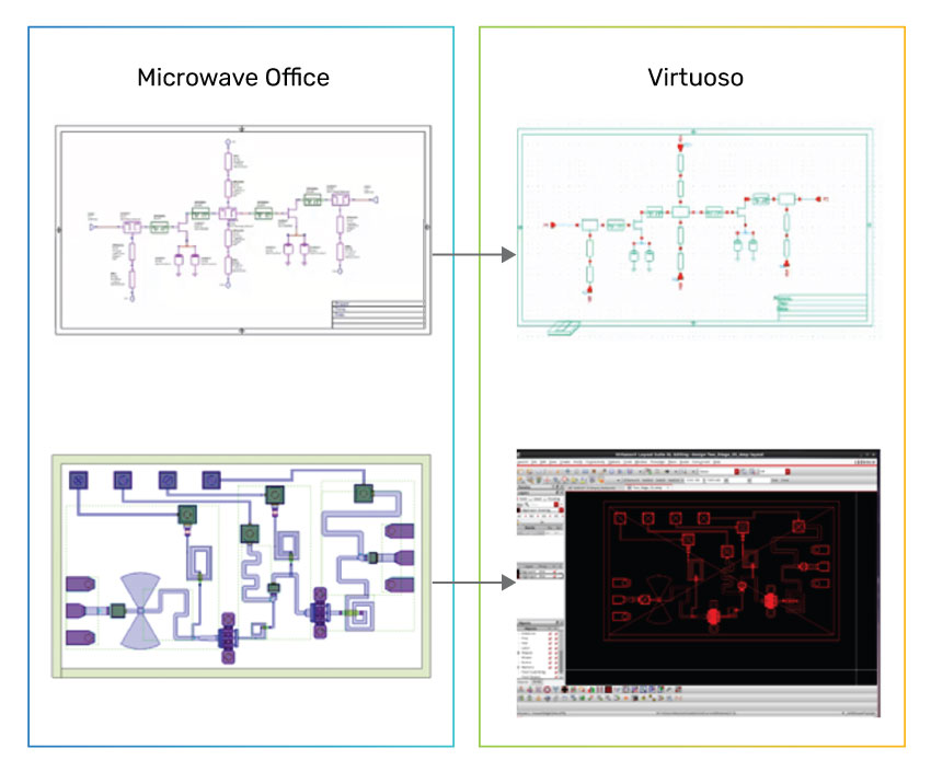
Microwave Office/Virtuoso Workflow
Export IP generated from Microwave Office software and implement it as MMIC or package/laminate technologies into Virtuoso Schematic Editor and/or Virtuoso Layout Suite to integrate these designs into multi-technology systems. The new interoperability eliminates the need for manual design re-entry, reducing time, costs, and the potential for errors. Schematic and layout sourced from Microwave Office software will have the same look and feel in the Virtuoso environment as the original design (Figure 3). Since most MMIC model and PCell libraries are defined and implemented by the III-V foundry as a process design kit (PDK), the Microwave Office MMIC design flow still utilizes this PDK for the target semiconductor process in the design.
The Spectre Simulation Platform can simulate RF IP based on Microwave Office software linear models, enabling co-design of RFICs, packages, and modules, inclusive of RF content such as off-chip matching and resonators. For example, Microwave Office software users can design passive off-chip components through circuit design, optimization, and EM verification, and then decide the best implementation technology. In some cases, a network of passive components may be more optimally implemented across the IC package boundary. This is often true for RF modules, where the ideal filter design, matching networks, and power amplifier (PA) output stage load termination often leverage components on both the die and in the package substrate.
Microwave Office/Allegro Workflow
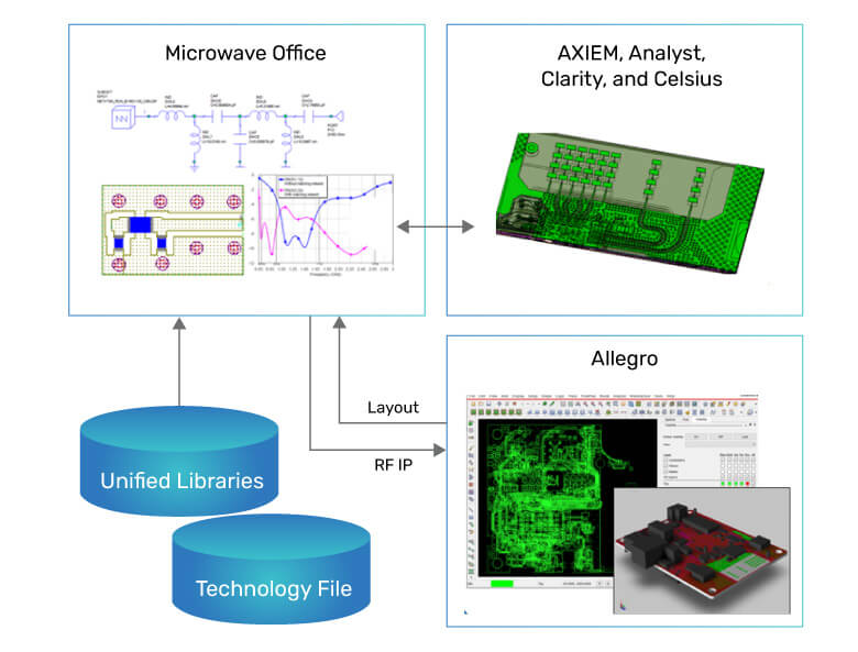
RF/microwave IP created and analyzed in Microwave Office software can be developed using Allegro libraries and technologies, ensuring compatibility with the Allegro PCB Designer schematic and layout editors, as well as the targeted manufacturing technologies using corporate-approved components. Using an organization’s approved bill of materials (BOM) eliminates the need to replace components in the RF design when edited inside the manufacturing framework. In addition, physical design constraints set in the Allegro platform are available within Microwave Office software for dynamic voiding of ground/power planes.
The Microwave Office to Allegro PCB workflow (Figure 4) provides a seamless schematic and layout data transfer from Microwave Office software to Allegro PCB Design platform, eliminating time-consuming and error-prone manual re-entry. By using parts with identical symbols, footprints, and properties between Allegro and Microwave Office software, RF designs are instantly recognizable to the layout engineer, allowing RF and layout design teams to work collaboratively, yet independently. The Allegro design can be imported back into the AWR Design Environment platform for high-performance, multiphysics analysis and design verification of the entire system after the RF IP has been incorporated with the rest of the PCB.
Microwave Office/High-Performance Multiphysics Analysis Workflow
Clarity 3D Solver Integration
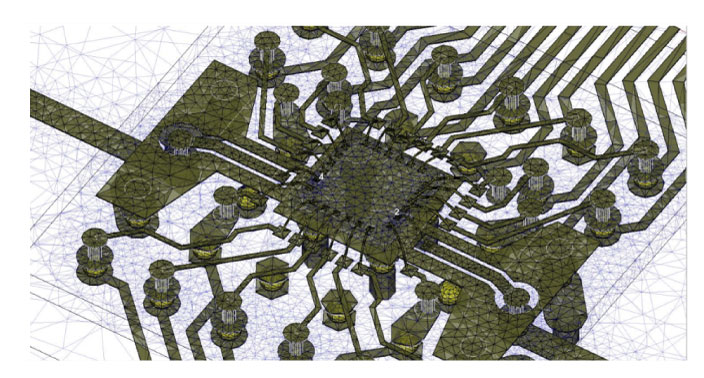
Large RF structures such as phased array feed networks are often manually sectioned into smaller structures for analysis using the largest and most powerful computing resources. The Clarity 3D Solver 3D EM simulator, used for designing critical interconnect, RFIC/MMIC, module, PCB, and SoIC designs, overcomes the limitations of legacy EM analysis software by leveraging Cadence’s distributed multiprocessing technology to deliver virtually unlimited capacity and 10X speed.
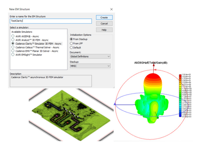
Now integrated within AWR software, the Clarity 3D Solver provides RF designers with ready access to high-capacity EM analysis for design verification and signoff of large, complex RF/ mixed-signal systems beyond the capabilities offered by the AXIEM 3D planar and Analyst 3D finite element method (FEM) solvers.
The Clarity 3D Solver integration with the Microwave Office software (Figure 5) is an automated process in which the entire analysis experience is fully within the AWR environment. Once the simulation is complete, a dataset with input geometry, simulation setup, and S-parameter results is automatically assembled and associated with the given EM document for plot/measurement and subsequent extraction, circuit simulation, tuning, and optimization. The link also supports mesh, current, and field visualization data in addition to S-parameters, enabling designers to take full advantage of the rich set of EM 3D annotations that already exist in the Microwave Office software.
Celsius Thermal Solver Integration
IC and electronic system companies, particularly those incorporating IC packaging and/or multi-technology modules, face tremendous thermal challenges that can cause late-stage design modifications and derail project schedules.
The Celsius Thermal Solver embedded within the Microwave Office software offers a solution (Figure 6) for RF PA and MMIC designs, RF PCBs, and modules, supporting electrothermal analysis through model information sourced from Microwave Office sofware’s project information, including existing MMIC (die or packaged device) design data and geometries such as layout, material properties, and powersource values from RF simulation. Celsius Thermal Solver structures can be created either by drawing/importing the geometry in the EM editor, or using EM extraction with simulated temperature results automatically returned into Microwave Office software.
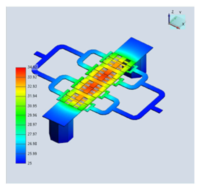
3D plots of the thermal temperature distribution can be viewed in the Celsius Thermal Solver native editor. For MMIC structures, the solver also provides a full-chip temperature profile at the relevant resolution of the IC layout, available as a graphically viewable 3D structure temperature overlay in the Celsius Thermal Solver’s native editor as well as a temperature-annotated netlist for circuit simulation.
| Additional Analysis and Productivity Enhancements | ||||
|---|---|---|---|---|
| Environment/Automation | Circuit Simulation | EM Simulation | System Simulation | Physical Design/Layout |
|
|
|
|
|