Technical Brief
EM Analysis: Why, When, and What?
Overview
Introduction
Cadence has multiple electromagnetic (EM) technologies within its product portfolio, some of which came via acquisition and others were created internally. With a wide breadth of EM simulation and analysis tools within the Cadence product families, you are likely asking yourself what you need to know about them and which one(s) to use.
Let’s start with what an EM solver does. First, it takes in a physical description of the conductors, typically layout, although for something like a connector it is actually a mechanical model.
Second, the EM solver processes the layout to get it into a form that can be used in the analysis phase. This typically involves “meshing” the conductors using the finite element method or something that is more optimized due to restrictions on the layout, such as it being planar. The meshing is required since all the analysis methods work on tiny pieces of the conductor where a lot of approximations can be made without significant error, and the overall analysis is done by assembling all of these little pieces of the puzzle into an overall solution.
So, for each element, the next phase is that the analysis is performed based on Maxwell’s equations for electromagnetism the solutions are combined to give a final result. The result of the analysis is provided as a model (such as S-parameters) that can be used in circuit simulation to verify performance.
Why and When to Do EM Analysis
There are two main reasons to do EM analysis: to see if the signals in the design will meet your performance specifications, and to see whether the design has unintended EM interactions in the circuit/system. In addition, there are different occasions on which you might want to do EM analysis.
The first scenario is when you are designing something (a chip, a package, a board, a system) and you want to see how good your current design is. You expect to look at the result of the analysis and then tweak whatever it is you are designing to further improve it. In this instance, you require high performance and integration. You want to go from your design system (a Cadence Virtuoso environment for chips, a Cadence Allegro environment for boards, perhaps third-party models for connectors) to results as fast as possible. You don’t want to have to manually transfer files, manually guide the meshing, and manually transfer the results back into your design environment. In fact, you don’t want to do anything manual at all, beyond clicking on a menu item to launch the analysis. Also, you are waiting while the analysis takes place, so you don’t want to wait a long time for the analysis—a few seconds would be great.
The second occasion for doing EM analysis is during signoff. You have finished your design, or at least you hope you have, and you want to get confirmation that it is as good as you can make it. In this case, you are less concerned about performance and more concerned about accuracy. Because you only plan on doing this analysis once, or at most only a few times, you don’t mind it being slow as long as you get numbers that are as close as possible to what you will eventually get once your design is manufactured/fabricated. In practice, it is less binary than design versus signoff and, as a design progresses, the tradeoff between runtime and accuracy changes continuously.
With those basics covered, which are common to all of the solvers, let’s take a look at Cadence’s EM technologies and understand more where they came from and the benefits of each.
Sigrity Technology
Cadence acquired Sigrity (the company) in 2012. There are various specialized options (such as Cadence Sigrity Serial Link Analysis) but here we’ll focus on the two that combine to give full EM analysis: Sigrity extraction technology and Sigrity Advanced SI technology. Sigrity technology is a planar 3D (sometimes called hybrid) solver, meaning that it uses a mostly 2D algorithm with lots of heuristics to deliver something close to the results you would get with a full 3D solver but much faster.
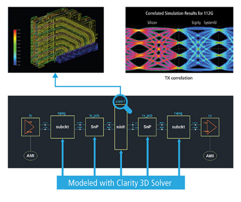
Clarity 3D Solver
The Cadence Clarity 3D Solver was developed internally and released in 2019. More information about the release is available in Bringing Clarity to System Analysis and a deeper dive can be found in Under the Hood of Clarity and Celsius Solvers.
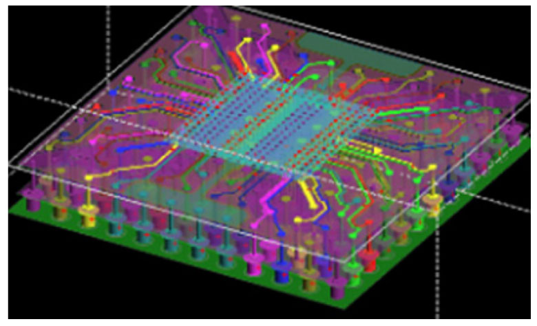
The Clarity 3D Solver is the most general of all the solvers and can handle arbitrary 3D structures. It is the tool of choice when full 3D analysis is required, or when none of the other solvers are appropriate, such as the analysis of a board and a connector or the analysis of a full ball-gridarray (BGA) package. It is also the most scalable of the solvers, having been designed from the start to run in large server farms and cloud data centers, without requiring enormous amounts of memory on any of the servers. Because of its capacity, this is considered system-level analysis. The only thing beyond the Clarity 3D Solver’s scope today is the type of analysis where you put an entire radar unit inside a chamber and analyze the signal from three meters away.
EMX Simulator
Cadence brought in the EMX 3D Planar Simulator through its acquisition of Integrand Software in 2020. More information about the acquisition can be found in Designing Radios: Integrand, more about their history and technology is available in The Integrand Story and you can take a deep dive into EMX in Analyzing On-Chip RF Passives.
EMX is optimized for analyzing passives on silicon. It is optimized for primarily planar conductors and small vias, just like on-chip interconnect. It also has a broad library of process design kits (PDKs) from all the major foundries. This combination means that it delivers quick and accurate results for on-silicon passives in foundry processes. But only for that special case. Luckily, that is a big special case since more and more passives are being moved on chip.
AWR AXIEM and Analyst Analysis
AWR AXIEM 3D Planar EM Analysis software was obtained when Cadence acquired AWR in 2020, although it was already being sold by Cadence through an OEM agreement. More information about the acquisition can be found in Cadence to Acquire AWR, as well as a deeper look at the technology in Designing Radios and Radar: AWR. It is optimized for use at the PCB level, and also for more general RF solution in the AWR Microwave Office software. AWR AXIEM analysis was integrated into Cadence’s Virtuoso RF Solution (at the source-code level) before the acquisition, as discussed in RF Design with Cadence Virtuoso and National Instrument’s AXIEM.
AWR EM technologies include AXIEM 3D Planar EM Analysis and Analyst 3D FEM EM Analysis. Both are tightly integrated into the Cadence AWR Design Environment platform that targets microwave applications from III-V chips to RF modules and even antennas. AWR AXIEM analysis is optimized for use at the planar structure level such as PCBs, MMICs, and the like. For more complex; designs that are multi-technology, such as a microwave/RF module or a system-level design that’s inclusive of a non-planar antenna, the Analyst software fits the bill.
Making a Choice
If you need a full 3D solver, either because the elements are not sufficiently planar or you are analyzing a large system, then the Clarity 3D Solver is the solution. If you are doing on-chip analysis (CMOS), then the EMX Simulator is the preferred EM solver. At the board and package level, Sigrity analysis, AWR AXIEM analysis, and Analyst software are all options and well-integrated into the Cadence platforms.
Learn More
Each of these solvers has a product page on the Cadence website:
-
 Sigrity Analysis Point Tools
 - Clarity 3D Solver
- EMX Planar 3D Simulator
- AWR AXIEM 3D Planar EM Analysis
- AWR Analyst 3D FEM EM Analysis