Success Story
EnSilica Design Services Tapeout in 12nm Using the Cadence Tempus Timing Solution and Tempus ECO

EnSilica is a leading fabless supplier of complex mixed-signal ASIC to OEMs and system houses. The company has world-class expertise in designing and supplying custom RF, mmWave, mixed-signal, and digital ICs to its international customers in the automotive, industrial, healthcare, and communications markets.
The Cadence Tempus Timing Solution and Tempus ECO enabled us to achieve our aggressive design services tapeout schedule. The tight integration between the Innovus Implementation System and Tempus Solution delivered a reduced number of closure iterations avoiding manual modification, reducing overall design closure time by 75%. This enabled us to get to market more quickly with the best-performing product.
Davide Sarta, VP SoC Engineering
Overview
Challenges
-
 7M instance flat implementation, 35mm2 in 12nm, 1GHz clock frequency
 - Multi-voltage implementation
- Timing closure with the existing tool flow is not converging quickly enough
- Unable to generate precise timing ECOs for all scenarios using the available resources, leading to additional iterations
- ECOs for timing do not consider physical and power domain constraints
Benefits
- Reduced final design closure iterations from 11 to 3
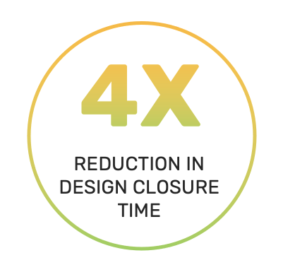
- Reduced time to close the design from 4 weeks to 1 week
- Physical design closure is predictable due to the close correlation between Innovus Implementation and Tempus Timing Solutions
- Automated distribution of concurrent timing analysis using distributed mode across a compute farm resulted in rapid turnaround times
- High quality of local support for the UK-based design team
Design
- High speed, high dependency data communication, and analysis SoC
Further Information
Learn more about Tempus Timing Solution.