- Overview
- Vision DSP Family Features and Benefits
- Vision 341 DSP Features and Benefits
- Vision 240 DSP Features and Benefits
- Vision 331 DSP Features and Benefits
- Vision 230 DSP Features and Benefits
- Vision 130 DSP Features and Benefits
- Vision 110 DSP Features and Benefits
- Vision 4DR Accelerator Features and Benefits
- Library Support
- Toolchain
- AI Software Support
- Cadence Services and Support
Product Overview
Tensilica Vision DSP and Accelerator Family
High-performance, low-energy camera, radar, lidar, and AI processing
The Cadence Tensilica Vision family is designed for demanding embedded vision, camera, radar, and artificial intelligence (AI) applications in the mobile, automotive, surveillance, augmented reality (AR) / virtual reality (VR), drone, and wearable markets. The six DSPs in the vision family offer 3.84 TOPS to 0.4 TOPS maximum performance. All Vision DSPs are built on the same VLIW SIMD architecture and offer an N-way programming model, allowing easy software migration from each DSP. All these DSPs offer the best DSP performance and the necessary MAC for today’s AI workload. Tensilica provides a comprehensive offering with low-end 128-bit SIMD, mid-range 512-bit SIMD, and high-end 1024-bit SIMD. These DSPs are also ISO26262-ready for the automotive market. Plus, as all our DSPs are built on the highly successful Cadence Tensilica Xtensa processor, the Vision DSP family shares the same development environment and can be extended using the Tensilica Instruction Extension (TIE).
In addition to programmable DSPs, the Vision family also offers a Vision 4DR Accelerator targeted at 4D Radar applications for automotive market, providing area, power, and performance advantage over a DSP-only solution.
Overview
Overview
For sufficient sensor data processing throughput, the Vision DSP product architecture incorporates advanced VLIW/SIMD support for the industry’s highest number of ALU and MAC operations per processor cycle and the industry’s widest and most flexible memory bus.
Specialized instructions also allow the Vision DSP products to efficiently speed up sensor data processing. Various architecture enhancements boost performance while keeping energy consumption low. The Vision DSP products provide unprecedented flexibility in system implementations at power-consumption levels that significantly reduce the need for hardware accelerators. The DSPs also offer an integrated DMA engine, an interface for instruction memory, an instruction cache, and two AXI interfaces. Vision 341 and 240 offer the industry’s widest data memory bus of 2048-bit. All DSPs also provide an optional vector floating-point unit supporting double, single-half precision, complex floating point, and bfloat16 operation. All Vision DSPs offer base-level AI accelerations on DSP by offering sufficient 4-bit, 8-bit, and 16-bit MAC acceleration.
Vision 341 and Vision 331 are the latest additions to the vision family and provide the best instruction set to run camera (vision), radar, lidar, and AI workload. Both these DSPs are built on the Xtensa NX controller, offering the best frequency possible. Vision 341 is a 1024-bit SIMD, and Vision 331 is a 512-bit SIMD. The newly introduced Vision 3xx family of DSPs offers the best architecture and instruction set for 4D imaging radar. For certain 4D imaging radar workloads, the 512-bit Vision 331 DSP offers up to 4X performance improvement over the Vision 230 DSP in radar boost mode, while the Vision 341 DSP offers up to 6X performance improvement over the Vision 230 DSP.
Vision 110 and Vision 130 provide a balanced architecture with optimum area, performance, and low energy. These DSPs are built on the latest Xtensa controller LX8, offering all new features for the best system design. Vision 110 with the 128-bit SIMD is the smallest Vision DSP, targeting lower power applications, offering one-third the power and area compared to Vision 130 while offering easy software transition from Vision 130 via the N-way programming model. Vision 110 also provides the flexibility to configure without various features to reduce area and the data RAM, providing the best area for on-sensor integration.
Both Vision 110 and Vision 130 offer the following improvements over previous generations of Vision P1 and Vision P6
-
 2X Floating-point performance
 - Up to 5X improvements on certain AI and Vision Kernel
- Floating FFT performance improvements
- Lower code size
|
|
Vision 110 |
Vision 130 |
Vision 230 |
Vision 331 |
Vision 240 |
Vision 341 |
Use Case |
|
|
|
|
|
||
MAX SIMD Width |
|
128 |
512 |
512 |
512 |
1024 |
1024 |
Xtensa Processor |
|
LX8 |
LX8 |
NX |
NX |
NX |
NX |
MAC For AI |
8x8 |
128 |
256 |
512 |
512 |
1024 |
1024 |
SHOW ALL
5 of 18
Table 1: Feature Summary
Vision 4DR Accelerator is the first accelerator product targeting 4D Imaging radar applications. As the automotive market moves to 4D radar that provides range, doppler, azimuth, and elevation information with large data cubes, it becomes challenging to implement the radar processing chain just in programmable DSPs. When paired with the new DSPs for 4D imaging radar applications, the Vision 4DR accelerator offers 4X greater performance and up to 6X greater area advantage than a Vision 341 DSP alone and 7X greater performance than a Vision 331 DSP alone.
Vision DSP Family Features and Benefits
- Provides high-performance, energy-efficient vision, and AI-embedded DSPs
- Implements 128-way 8-bit SIMD with multiple VLIW slots on Vision 240 and Vision 341
- Implements 64-way 8-bit SIMD with multiple VLIW slots on Vision 331, Vision 230, Vision 130
- Implements 16-way 8-bit SIMD with multiple VLIW slots on Vision 110
- Vision 110/130 DSP achieves up to 1.1GHz on 16nm process technology
- Vision 341/240 and Vision 331/230 DSP achieve up to 1.5GHz on 16nm process technology
- Vision 341/240 offers a 2048-bit memory bus for transferring high-resolution data associated with today’s imaging systems
- Vision 3xx family can boost radar and computer vision performance with Instruction Set improvements and offers power and area-optimized 4D Imaging radar with Radar Turbo Mode in conjunction with the Vision 4DR Accelerator.
- Provides a complete subsystem using the integrated DMA with 128-and 256-bit AXi interface that allows the system to transfer high-resolution data directly into the local memory of the DSP, thus hiding the data access latency associated with accessing data from an external DRAM.
- Implements the Tensilica SuperGather enhanced memory interface to read/write non-contiguous locations from local memory quickly and efficiently.
- Features an instruction set customized for better code density, fewer cycles, and lower power.
- The Vision DSP family delivers scalable, optimized performance with low energy for computer vision and pixel-processing applications that span a large range of data types from 8b to 32b, such as face detection, object detection, lens distortion correction, and many more advanced vision applications.
- Optional vector floating-point unit (VFPU) in the Vision DSP family provides high-precision math with minimal area penalty.
Vision 341 DSP Features and Benefits
- Single DSP for Vision/Radar/Lidar and Ai
- The Cadence Tensilica Vision 341 DSP is a 1024-bit SIMD DSP offering a single DSP for vision, radar, lidar, and AI. To address the increasing computational requirements for embedded vision, radar, lidar, and AI applications, the 1024-bit Vision 341 DSP provides up to 6X greater FFT performance than the Vision 230 DSP, and due to the single DSP with support for both vision and radar, it also offers tremendous area, power, and cost saving. It can also connect to the Vision 4DR Accelerator to provide a high-resolution imaging radar solution.
- The Vision 341 DSP delivers up to 3.84 tera operations per second (TOPS). To address the increasing computational requirements for embedded vision and AI applications, the Vision 341 DSP provides up to 2X greater AI and floating-point performance than the Vision 230 and Vision 331 DSP. The Vision 341 DSP also brings the next-generation simultaneous localization and mapping (SLAM) acceleration, a technique commonly used in the robotics, drone, mobile, and automotive markets to automatically construct or update the map of an unknown environment, and in the AR/VR market for inside-out tracking.
- While considering AI acceleration, the Vision 341 DSP also offers acceleration for non-convolution layers. Special enhancements are provided to improve the performance of high-level languages such as OpenCL and Halide.
- An enhanced instruction set supporting 8/16/32-bit data types and optional VFPU support for double, single, and half-precision enable up to 2X faster performance on SLAM kernels than the Vision 230 DSP. the Vision 341 DSP supports complex floating point and special enhancements for FFT.

Figure 1: Vision 341 Block Diagram
Vision 240 DSP Features and Benefits
- Offers 1024 8-bit MAC
- The Vision 240 DSP delivers up to 3.84 tera operations per second (TOPS). Vision 240 is the first 1024-bit SIMD DSP from Cadence. To address the increasing computational requirements for embedded vision and AI applications, the seventh-generation Vision 240 DSP provides up to 2X greater AI and floating-point performance than the Vision 230 DSP. The Vision 240 DSP also brings the next-generation simultaneous localization and mapping (SLAM) acceleration, a technique commonly used in the robotics, drone, mobile, and automotive markets to automatically construct or update the map of an unknown environment, and in the AR/VR market for inside-out tracking.
- While considering AI acceleration, the Vision 240 DSP also offers acceleration for non-convolution layers. Special enhancements are provided to improve the performance of high-level languages such as OpenCL and Halide.
- An enhanced instruction set supporting 8/16/32-bit data types and optional VFPU support for double, single, and half-precision enable up to 2X faster performance on SLAM kernels than the Vision 230 DSP. For the first time in the Vision DSP product line, the Vision 240 DSP supports complex floating point and special enhancements for FFT.
- Delivers up to 2X improvement in floating-point operations per mm2 (FLOPS/mm2) for double, single-precision (FP32), and half-precision (FP6) than the Vision 230 DSP.
- It has up to 2X greater AI performance than the Vision 230 DSP with 1024 8-bit and 256 16-bit MAC.

Figure 2: Vision 240 Block Diagram
Vision 331 DSP Features and Benefits
- Offers 512 8-bit MAC
- The Cadence Tensilica Vision 331 DSP is a 512-bit SIMD DSP offering a single DSP for vision, radar, lidar, and AI. To address the increasing computational requirements for embedded vision, radar, lidar, and AI applications, the 512-bit Vision 331 DSP provides up to 4X greater FFT performance than the Vision 230 DSP, and due to the single DSP with support for both vision and radar, it also offers tremendous area, power, and cost saving. It can also connect to the Vision 4DR Accelerator to provide a high-resolution imaging radar solution.
- An enhanced instruction set supporting 8/16/32-bit data types and optional VFPU support for single and half-precision enables up to 2X faster performance on SLAM kernels than the Vision 130 DSP.
- Delivers up to 2X improvement in floating-point operations for both half-precision (FP16) and single precision (FP32) than the Vision 130 DSP.

Figure 3: Vision 331 Block Diagram
Vision 230 DSP Features and Benefits
- Offers 512 8-bit MAC
- The Vision 230 DSP delivers up to 2.18 tera operations per second (TOPS), 2.565X higher total TOPS than Vision 130. To address the increasing computational requirements for embedded vision and AI applications, the sixth-generation Vision 230 DSP provides up to 2X greater AI and floating-point performance than the Vision 130 DSP. The Vision 230 DSP is specifically optimized for simultaneous localization and mapping (SLAM), a technique commonly used in the robotics, drone, mobile, and automotive markets to automatically construct or update the map of an unknown environment and in the AR/VR market for inside-out tracking.
- An enhanced instruction set supporting 8/16/32-bit data types and optional VFPU support for single and half-precision enables up to 2X faster performance on SLAM kernels than the Vision 130 DSP.
- Delivers up to 2X improvement in floating-point operations for both half-precision (FP06) and single precision (FP32) than the Vision 130 DSP.

Figure 4: Vision 230 Block Diagram
Vision 130 DSP Features and Benefits
- Offers 256 MAC
- Vision 130 follows the highly successful Vision P6 introduced in 2016 and the first Vision DSP to offer 256 MAC. With a balanced architecture offering optimum area, performance, and low energy, it is one of the most successful vision DSPs in the market. Vision 130 is built on the latest Xtensa LX8 controller, offering various system-level improvements to the Vision DSP.
- It is used in mobile, automotive, surveillance, and AR/VR market products to process sensor data or also used as a DSP next to NPU for future AI workloads.
- Enhanced instruction set for computer vision and AI.
- Smart instruction slotting.
- Supports SuperGather enhanced memory interface.
- Optional VFPU with single-precision (32-bit) floating-point and half-precision (16-bit) floating-point support offers the flexibility to port GPU code and high-precision math at a minimal area penalty.

Figure 5: Vision 130 Block Diagram
Vision 110 DSP Features and Benefits
- Offers 128 8-bit MAC
- Vision 110 is the latest addition to the Vision DSP family. The smallest Vision DSP targets lower power always -application offering one-third the power and area compared to the highly successful Vision 130 while providing easy software transition from Vision 130 via the N-way programming model. Vision 110 also provides the flexibility to configure without various features to reduce area and the data RAM, providing the best area for on-sensor integration.
- Optional VFPU with single-precision (32-bit) floating-point and half-precision (16-bit) floating-point support offers the flexibility to port GPU code and high-precision math at a minimal area penalty.

Figure 6: Vision 110 Block Diagram
Vision 4DR Accelerator Features and Benefits
The Cadence Tensilica Vision 4DR Accelerator is hardware designed to address the increasing computational requirements for 4D Imaging radar in the automotive market. With its much higher performance than a DSP-only solution, a combined solution of Vision 331/341 with Vision 4DR saves considerable power and area.
- Accelerates 2D and 1D Fast Fourier Transform (FFT) commonly used in Radar processing
- 16/24-bit fixed-point processing
- Programmable input scaling
- AXi-based IP with multiple DMA (128/256-bit) for fast data movement
- Highly programmable: ability to select data width, windowing, FFT size
- System software to work as FFT offload engine for Vision 331/341
- ISO 26262 ready for automotive market
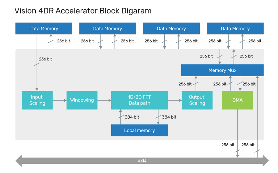
Figure 7: Vision 4DR Accelerator Block Diagram
Library Support
- Vision 110, 130, 230, 240, 331, and 341 DSPs offer highly optimized OpenCV-based library functions, SLAM library, Radar Library, and Nature DSP Library, which can accelerate application development.
- Vision 110, 130, 230, 240, 331, and 341 DSPs offer a highly optimized NN library.
Toolchain
The Vision DSPs are delivered with a complete set of software tools:
- A high-performance C/C++ compiler with automatic bundling and vectorization supports the VLIW and SIMD capabilities.
- Linker, assembler, debugger, profiler, and graphical visualization tools are included.
- A comprehensive instruction set simulator (ISS) lets you quickly simulate and evaluate performance.
- When working with large systems or lengthy test vectors, the fast, functional TurboXim simulator achieves 40X to 80X faster speeds than the ISS for efficient software development and functional verification.
- Tensilica Xtensa Modeling Protocol (XTMP) for system modeling in C and Xtensa SystemC (XTSC) for system modeling in SystemC® enable full-chip simulations. The pin-level XTSC model offers co-simulation of the SystemC model at the pin level for fast, cycle-accurate system simulations.
AI Software Support
- All Vision DSPs support the Tensilica Neural Network Compiler (NeuroWeave), which maps any neural network trained with a framework such as Caffe, TensorFlow, and TensorFlow Lite into executable and highly optimized fixed-point code for target DSPs, leveraging a comprehensive set of hand-optimized neural network library functions.
- Vision 130 and 110 also support TFLiteMicro for always-on applications.
- High-Level Language Support
- All Vision DSPs support OpenCL and Halide compiler for the rapid development of computer vision and imaging applications using high-level languages.
- Supports all major back-end EDA flows