- New Features of Xtensa LX7 Processors
- General Features of LX7 Processors
- Benefits
- Xtensa LX7 Processors for Today’s SoC Challenges
- Efficient Base Architecture
- New Xtensa LX7 Processor Features and Options
- Add Flexibility and Extensibility to SoC Designs with Xtensa Processors
- Xtensa LX7 Processor as an RTL Companion
- Extending the Life of an Existing RTL Design
- Rapid Design Development, Simulation, Debug, and Profiling
- Hardware Development
- Software Development
- Specifications
- Cadence Services and Support
Datasheet
Xtensa LX7 Processor
High-performance, configurable, and extensible controllers and DSPs
Cadence provides system-on-chip (SoC) designers with the world’s first configurable and extensible processor, fully supported by automatic hardware and software generation. Cadence Tensilica Xtensa processors enable SoC designers to add performance, flexibility, and longevity to their designs through software programmability, as well as differentiation through processor implementations tailored for their specific application. Xtensa LX7 processors and digital signal processors (DSPs) can be configured and customized to cover a vast array of SoC functions, including embedded controllers, powerful audio, communications, and vision DSPs, and specialized custom cores for security and network processing.
Overview
New Features of Xtensa LX7 Processors
General Features of LX7 Processors
Benefits
Xtensa LX7 Processors for Today’s SoC Challenges
Inside today’s complex SoCs, you can find many different processors, from general-purpose processors to function-specific offload DSPs, that add programmability and flexibility. Although general-purpose embedded processors can handle most of the control tasks well, they lack the architecture, features, or bandwidth needed to perform complex, data-processing tasks such as network or baseband packet processing, image processing, audio processing, and digital cryptography.
Chip designers have long turned to hardwired logic (blocks of RTL) to implement these key functions. The problem with the RTL blocks is that they take too long to design, take even longer to verify, and are not programmable or flexible.
Xtensa LX7 processors are configurable and extensible and ideal for handling complex compute-intensive digital signal processing applications where a fixed register-transfer level (RTL) implementation may be the only other option.
Xtensa ISA Feature Overview
Efficient Base Architecture
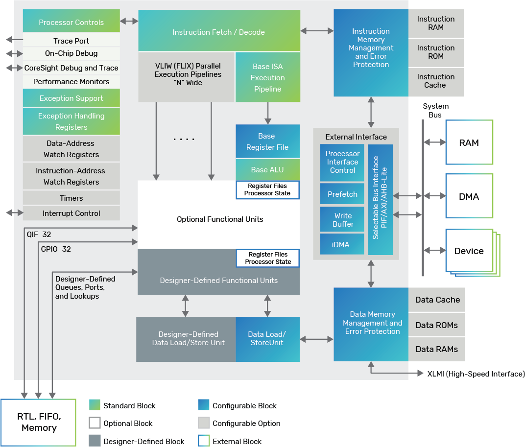
The Xtensa LX7 processor’s 32-bit architecture (Figure 1) features a compact instruction set optimized for embedded designs. The base architecture has a 32-bit ALU, up to 64 general-purpose physical registers, 6 special-purpose registers, and 80 base instructions, including 16- and 24-bit (rather than 32-bit) RISC instruction encoding. Key features include:
Base ISA compatibility
Configurability of an Xtensa processor core builds on the underlying base Xtensa ISA, thereby ensuring availability of a robust ecosystem of third-party application software and development tools. All configurable, extensible Xtensa processors are compatible with major operating systems, debug probes, and ICE solutions. For each processor, the automatically generated, complete software-development tool chain includes an advanced IDE based on the Eclipse framework, a world-class C/C++ compiler, a cycle-accurate SystemC-compatible instruction set simulator (ISS), and the full industry-standard GNU tool chain.
The Xtensa ISA includes powerful compare-and-branch instructions and zero-overhead loops, which allow the compiler to generate tight, optimized loops. It also provides bit manipulations, including funnel shifts and field-extract operations that are critical for applications such as networking, that process the fields in packet headers and perform rule-based checks.
Extensible ISA
One of the fundamental technology innovations in the Xtensa processor is the ability to easily and seamlessly add instructions into the processor’s data path. Any associated C data types, the software tool chain support, and the EDA scripts required to synthesize the processor are all generated automatically, just as if they had been there from the start. The specification of this data path and associated instructions and C data types is written in the TIE language, which is explained in more detail in a later section.
Highly configurable functionality
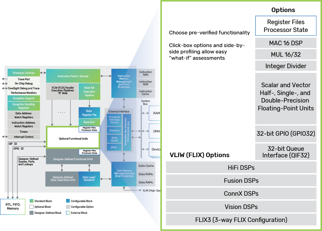
Xtensa processors offer pre-verified options that you can add to your designs when they are needed. Select from click-box options to add functionality to your processor and evaluate performance improvements quickly.
Basic Xtensa LX7 processor options include:
Configurable ISA options
Highly configurable interfaces
Dynamic and leakage power improvements
Multi-core design style support
Multi-core debug and ease of use
Natural connectivity with RTL, processors, or peripheral blocks
Complete hardware implementation and verification flow support
High-speed, high-accuracy system-simulation models automatically created
Xtensa Xplorer IDE
Robust real-time operating system support
Additional pre-verified optional DSP execution units
New Xtensa LX7 Processor Features and Options
Low-latency iDMA controller
iDMA Benefits
Enhanced AXI4 bus interface with ACE-Lite, Exclusive Access, Security, and ECC support
Enhanced features that support functionally safety and ISO 26262 compliance
Scatter-gather feature available on select DSPs, improving non-uniform accesses algorithms
Fine-grained MPU (Table 1)
| Feature | Region Protection Unit | MMU (Linux) | Memory Protection Unit |
|---|---|---|---|
| Granularity | 512MB regions | 4KB pages | Variable-size segments (4KB - 1GB) |
| Virtual address translation | N | Y | N |
| Number of elements | 8 regions | No. of pages set by page tables | 16 or 32 foreground segments |
| Privleged access modes | N | 4 | User/kernel |
| Memory attributes | 4 | 4 | 9 |
| Access control | N | Per page table entry | 12 access types |
| Organization | Split I/D | Split I/D | Unified I/D |
Table 1: Memory protection options available in the Xtensa LX7 processor
Add Flexibility and Extensibility to SoC Designs with Xtensa Processors
General-purpose processors offer limited flexibility with options for memory size, cache size, and bus interface. Performance is generally proportional to the clock speed. Beyond that, application code optimization or a move to the next-generation processor is required to get incremental performance benefits.
Cadence offers SoC designers the unique ability to add flexibility and longevity to their designs through software programmability as well as differentiation through processor implementations tailored for the specific application. You can now design a processor whose functions, especially its instruction set, can be extended to include features never considered or imagined by designers of the original processor, all using the TIE language.
The TIE language can be used to describe instructions, registers, execution units, and I/Os that are then automatically added to the processor. The TIE language is a Verilog-like language used to describe desired instruction mnemonics, operands, encoding, and execution semantics. TIE files are inputs to the Xtensa Processor Generator. The generator automatically builds the processor and the complete software tool chain that incorporates all configuration options and new TIE instructions. The base instruction set remains for maximum compatibility with third-party development tools and operating systems.
The TIE language unlocks the true power of the Xtensa processor. It lets you get orders of magnitude performance increases for your applications and create differentiation. Extensibility with Xtensa processors allows features to be added or adapted in any form that optimizes the processor’s cost, power, and application performance.
Flexibility—Add just what you need
Just as you can choose from a set of predefined functional options to improve processor performance, you can now create instructions that can speed up standard or proprietary algorithms, and scale data interfaces for greater bandwidth. Using the tools provided, application hot spots can be identified and additional instructions created to process these hot spots more efficiently, without the need to increase the clock frequency or re-write a lot of the software.
Differentiate—Make a processor that’s uniquely your own
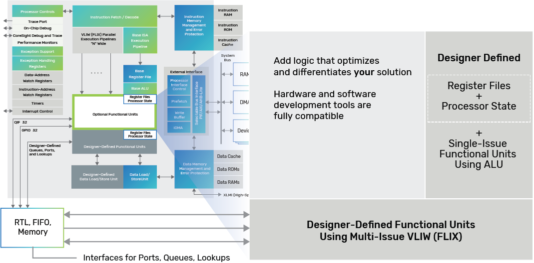
With fixed-function general-purpose processors, differentiation is often limited to the algorithm implementation itself. General-purpose processors are good at general-purpose computing, but not so good at any specific algorithm. Xtensa processors give you the opportunity to differentiate by implementing algorithms more efficiently with hardware that accelerates your particular algorithm (Figure 3). This means that your design will be almost impossible to copy, as only your custom processor will reach the performance required on the same software implementation.
FLIX for parallel execution
Many of the major pre-configured functional blocks take advantage of the Xtensa LX7 processor’s FLIX capabilities.
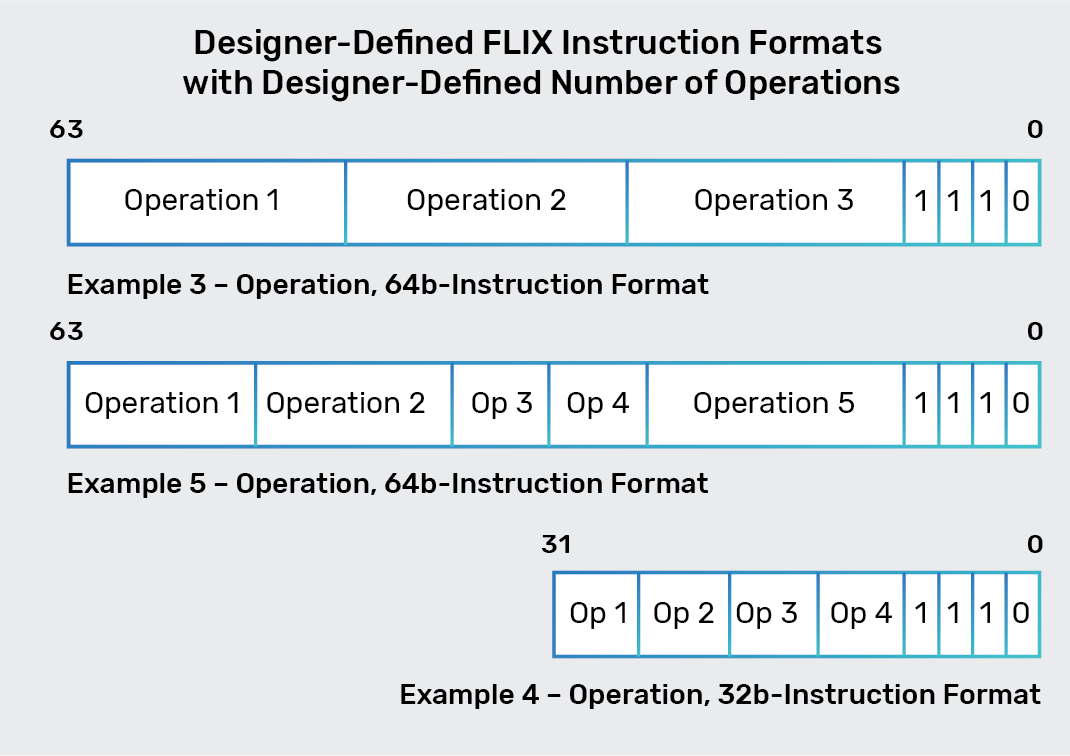
The FLIX architecture makes the Xtensa LX7 processor into a VLIW processor that executes 2 to 30 parallel execution units when needed. FLIX instructions can be as small as 4 bytes, as large as 16 bytes, or any size in between. These variable-width FLIX instructions are seamlessly intermixed with the base Xtensa 16/24-bit instructions, so there is no mode switch penalty when using FLIX (Figure 4).
Designer-defined I/Os bypass the system bus for maximum data throughput
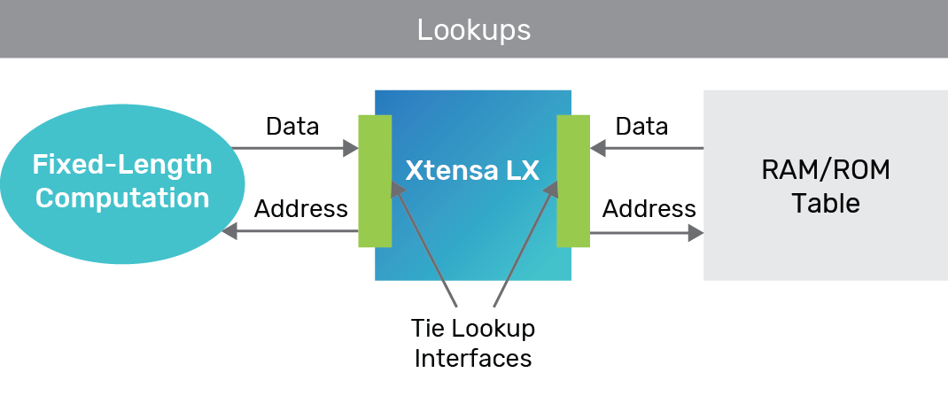
Xtensa processors bring another fundamental breakthrough in embedded processor designs—the ability to define direct data interfaces into and out of the processor for maximum data throughput. This ability is a key reason that Xtensa processors are ideal for the SoC data processing. Xtensa processors provide three direct interface capabilities:
Port connections can be up to 1024 wires wide, allowing wide data types to be transferred easily without the need for multiple load/store operations. As many as one million signals (1000 1024-bit-wide ports) can be used. While this number far exceeds the performance demands of real systems today, this clearly demonstrates that the conventional I/O bottlenecks inherent in a system-bus-based solution do not apply to Xtensa processors.
While ports are ideal to quickly convey control and status information, queues provide a high-speed/low-latency mechanism to transfer streaming data with buffering. Input queues and output queues operate, to the programmer’s viewpoint, like traditional processor registers—without the bandwidth limitations of local and system memory accesses.
TIE port and queue wizard
As shown in Figure 5 and Figure 6, the Xtensa Xplorer IDE provides a wizard for quickly generating ports and queues without the need to write any TIE code.
Xtensa LX7 Processor as an RTL Companion
RTL verification has become the most resource- and time-consuming aspect of SoC design. Xtensa processors offer unique advantages to SoC designers where they can use a pre-verified IP core as a foundation and add custom extensions through correct-by-construction design techniques. This design approach significantly reduces the need for the long verification times required when designing custom RTL. Xtensa processors can connect directly to your RTL with dedicated high-bandwidth data and control interfaces.
Bandwidth of hard-wired logic and performance without hand-coded state machines
The Xtensa processor can achieve virtually the same levels of inter-block I/O bandwidth and intra-block computational parallelism as hard-wired logic designed with traditional RTL design methodologies. How? By using a combination of TIE ports and queues, parallel FLIX execution units, and some TIE instructions.
Unlike RTL-based designs, Xtensa processors are pre-verified, and do not require hard-wired implementation of complex state machines. Instead of state machines, the datapaths are sequenced and controlled by the processor’s instruction stream. That means the “control logic” is fully programmable and can be debugged using software development methodologies, thereby reducing verification time and risk for the entire SoC.
Lower verification effort and time
Designing hardwired RTL blocks has become more about verification than about design. Design teams typically spend twice the number of resources and person months on verification than on design. Design changes made late in the project cycle are often limited by the verification effort.
Typically, 90% of the RTL block’s area lies in the datapath and only 10% in the control logic, yet most (perhaps 90%) of the bugs are found in the control logic. The ability to extend the Xtensa processor using TIE specifications enables designers to create datapaths inside the processor without the need to generate and verify the associated control logic. Instead, the control logic is expressed in software as instructions that execute on the processor.
It is easier to verify TIE specifications made to the Xtensa processor than it is to verify an equivalent RTL datapath, since only the I/O relationship and functional behavior of the operations specified in TIE code have to be verified. The TIE Compiler and Xtensa Processor Generator take care of converting the TIE specification into data path elements in the processor pipeline and implementing the control, decode, and bypass logic in the processor control units.
Reuse of the same hardware for multiple tasks
Complex SoCs consist of millions of gates of logic and are designed to perform multiple tasks. Often these multiple tasks do not need to be performed at the same time. This provides an opportunity for multiple tasks to share the same hardware units. Processors are particularly amenable to enabling this type of sharing.
Designers can specify a datapath in the TIE specification that consists of a set of execution units that can be used by multiple tasks and then use the programmability of the processor to determine which tasks are executed. For example, an audio engine can be designed to implement a range of audio codecs, such as MP3, AC-3, WMA, etc.
Flexibility to fix and upgrade algorithms post-silicon
An Xtensa processor implementation of an algorithm lets the designer fix, enhance, and tweak the algorithm even after the SoC has taped out. In particular, post-silicon bugs now have a chance of being worked around. Algorithms that are subject to continuous research, such as half-toning in printers and image and video post-processing, are ideal candidates for implementation in an Xtensa processor. Using Xtensa processors, you can easily add functionality to an existing design, or upgrade parts of it to support the latest standard, with limited development effort.
Co-simulation at the RTL pin level
Connect directly to your RTL wires using pin-level XTSC SystemC model interfaces without the need to purchase additional EDA vendor tools. This enhancement to transaction-level XTSC models allows designers to interchange SystemC and RTL blocks for co-simulation. This works with all of the major EDA vendor simulation tools.
Extending the Life of an Existing RTL Design
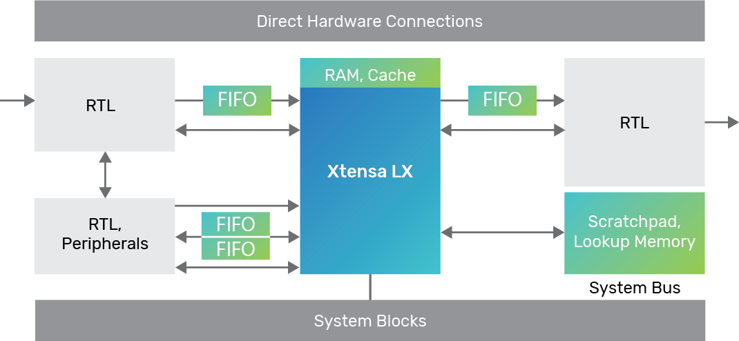
Using Xtensa processors, you can easily add functionality to an existing design, or upgrade parts of it to support the latest standard, with modest development effort. As with any other 32-bit processor core, all communication is through the system bus (Figure 7), which must have the available data bandwidth and must keep bus latency manageable.
Add functionality with Xtensa processors
With Xtensa processors, data can be kept off the system bus by using direct connectivity to RTL through ports and queues (Figure 8). These provide almost unlimited bandwidth with precise latencies.
When extending the functionality of existing RTL blocks, the control logic parts can be brought into the processor to make the FSM easier to debug and verify (Figure 9).
The datapath of the existing RTL module can also be brought into the processor as a datapath extension to create a highly optimized solution (Figure 10).
Rapid Design Development, Simulation, Debug, and Profiling
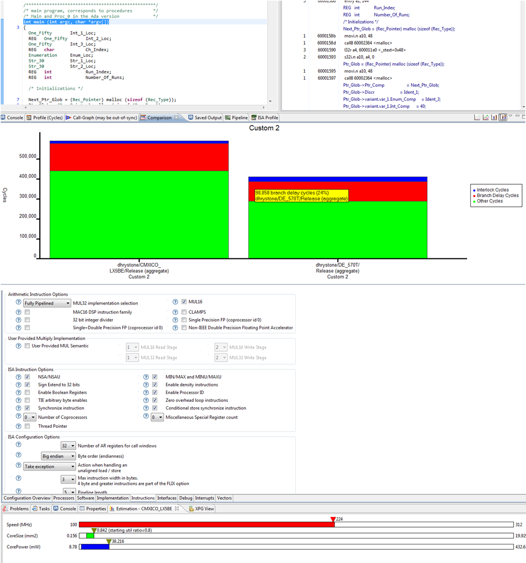
The Xtensa Xplorer IDE serves as the graphical user interface (GUI) for the entire design experience. From the Xtensa Xplorer IDE, designers with existing application software can profile their application, identify hot spots, decide on configuration options, add instructions and execution units to optimize performance, and then generate a new processor—all within a matter of hours. No other IP provider puts such flexibility directly into the hands of the designer with a tool that integrates software development, processor optimization, and multi-processor SoC architecture in one IDE.
Hardware designers now have creative options for implementing algorithms. Interfaces can be added to the processor to offer direct, deterministic connectivity to SoC logic. With the customizable port and queue interfaces, designers can stream data into or out of the processor. This direct connectivity with the rest of the SoC offers great control and predictable bandwidth. The simple ‘C’ programs needed to control the Xtensa processor can be written and debugged within the Xtensa Xplorer IDE.
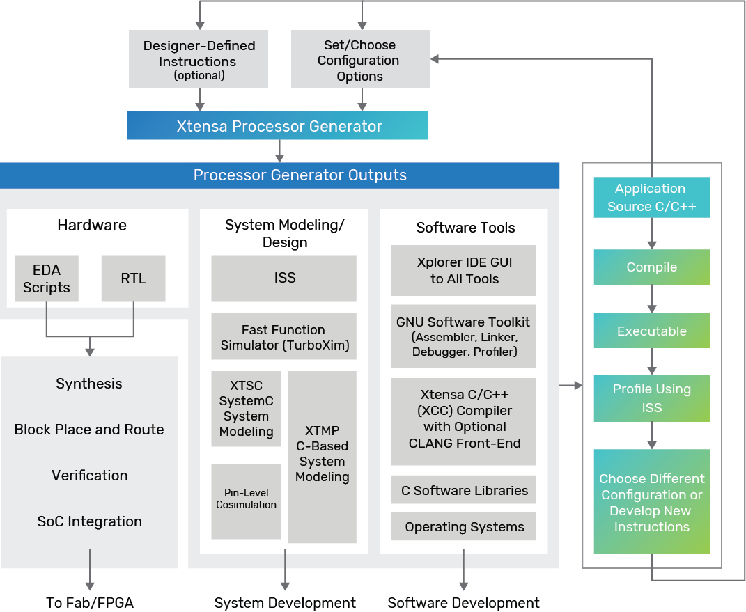
The Xtensa Processor Generator (Figure 11) creates a complete hardware design with matching software tools, including a mature, world-class compiler, a cycle-accurate SystemC-compatible ISS, and the full industry-standard GNU tool chain.
Hardware Development
Hardware designers can profile, compare, and save many different processor configurations. Use the ISS to simulate a single processor or, for multi-processor subsystems, choose Cadence’s XTensa Modeling Protocol (XTMP) or XTSC modeling tools.
The Xtensa Xplorer IDE (Figure 12) serves as the gateway to the Xtensa Processor Generator. Once a processor configuration is finalized, the Xtensa Processor Generator creates the automatically verified Xtensa processor to match all of the configuration options and extensions you have defined, in about an hour. The full software tool chain is also created that matches all processor modifications made. (See the Processor Developer’s Toolkit product brief for more information.)
Complete hardware implementation and verification flow support
Software Development
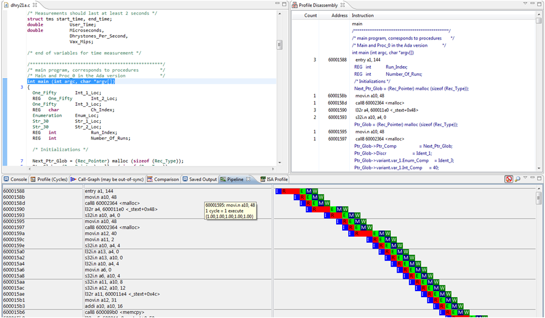
The Xtensa Software Developer’s Toolkit (SDK) provides a comprehensive collection of code generation and analysis tools that speed the software application development process. The Eclipse-based Xtensa Xplorer GUI (Figure 13) serves as the cockpit for the entire development experience and also provides powerful visualization tools to aid application optimization.
The entire Xtensa software development tool chain, along with simulation models, RTOS ports, optimized C libraries, etc., are automatically generated by the Xtensa Processor Generator. This also ensures that all the software tools—such as the compiler, linker, assembler, debugger, and ISS—always match and are tuned exactly to any custom processor hardware.
Complete software development tools
Ideal for applications where low power is critical
Power often is the key issue in a SoC design. Many techniques are employed to reduce power consumption, both built in to the base hardware and into the configuration options, allowing more control over system and memory resources. Xtensa processors consistently consume less power than other licensable embedded CPUs at equivalent gate counts.
Insertion of fine-grained clock gating for every functional element is automated, including those defined by the designer. This automation gives the Xtensa processors a significant advantage over RTL design where manual, error-prone post-layout tuning of clock circuits is often required.
Accessing local memories is one of the highest power-consuming activities. Xtensa LX7 processors eliminate any unnecessary local memory interface activation if that memory is not directly addressed by the processor. With Xtensa LX7 processors, you can now do semantic and memory data gating to save dynamic power.
Caches are other blocks that may consume significant power. Xtensa LX7 processors allow caches to be implemented at configuration time, and provide a way to shut down parts of the cache to match the operating load on the processor.
A programmer can turn off one, two, three, or all four of the cache “ways” to reduce dynamic power usage during idle or low-load periods, and turn them on again when they are needed.
As process geometries shrink, leakage power consumes a larger portion of the total power budget. To substantially reduce leakage power, Xtensa LX7 processors give you power-saving options during processor configuration. Implementation of the following energy-saving techniques is automated by the Xtensa Processor Generator:
The designer can configure the external data bus width and internal local memory data widths independently. This allows system-level power optimizations depending on whether the processor is constrained by external or internal instruction and data access.
Multi-processor features and debug options
Placing multiple processors on the same IC die introduces significant complexity in SoC software debugging. All versions of the Xtensa processor have certain optional PIF operations that enhance support for multi-processor systems. The Xtensa processor’s debug features include:
Access to these debug functions is:
Some SoC designs use multiple Xtensa processors that execute from the same instruction space. The processor ID option helps software distinguish one processor from another via a PRID special register.
The break-in/break-out option for the Xtensa Debug Module simplifies multi-core debugging. This capability enables one Xtensa processor to selectively communicate a break to other Xtensa processors in a multiple-processor system. A DebugStall feature allows Xtensa processors to be stopped and started together using a hardware signal and to be debugged while in the stalled state.
In addition to multi-processor debug, it is also possible to non-intrusively trace multiple processors if they are configured with the trace extraction and analysis tool, TRAX. TRAX, which is detailed in the Debug Guide, is a collection of hardware and software components that provides visibility into the activity of running processors using compressed execution traces. The ability to capture real-time activity in a deployed device or prototype is particularly valuable for multi-processor systems where there are a large number of interactions between hardware and software.
When multiple processors are used in a system, some sort of communication and synchronization between processors is required. The Xtensa Multiprocessor Synchronization configuration option provides ISA support for shared-memory communication protocols.
The Performance Monitor module is used to count performance-related events, such as cache misses. Accessing the counts through JTAG or APB is non-intrusive, but it is also possible to configure an interrupt to software running on an Xtensa processor.
Specifications
Because it is highly customizable, an Xtensa processor can run very efficiently at low MHz and very fast at clock frequencies over 1GHz. Maximum achievable clock speeds vary with the choice of process technology, cell library, feature set, and EDA optimization techniques.
The latest EDA tools, process flows, and other input are tracked to provide detailed performance information. For the latest data, please contact your local representative.

