Legato Reliability Solution

Industry’s first complete analog IC design-for-reliability solution

The Cadence Legato Reliability Solution provides analog designers with the tools they need to manage their design’s reliability throughout the product lifecycle. Responding to the challenges of designing for mission-critical applications such as automotive, aerospace, and medical design, the Legato Reliability Solution includes new technology to simulate the manufacturing test’s ability to identify and eliminate defective parts, the effect of temperature on circuit electrical performance, and changes in devices over time including the effects of temperature and process variation on aging.

Overview

The Legato Reliability Solution addresses the challenges and evolving product lifecycle requirements of mission-critical systems such as automotive, medical, aerospace and defense, and communications. The Legato Reliability Solution targets three key issues designers face: how to eliminate early failures due to test escapes, how to ensure devices survive in extreme operating conditions, and how to extend product life. Analog defect simulation allows designers to simulate their designs with manufacturing defects to ensure the test eliminates bad dies. Electrothermal simulation allows designers to simulate the effect of extreme operating conditions on a circuit’s dynamic performance. And advanced aging analysis allows designers to include the effects that accelerate aging in the analysis.

Key Benefits

  • Analyzes test coverage of manufacturing test using analog defect simulation
  • Advanced aging analysis for better prediction of device operating lifetime
  • Performs dynamic electrothermal simulation of design to prevent thermal overstress during operation
  • Analog defect simulation is integrated into the Spectre AMS Designer to enable simulation of mixed-signal designs
  • Based on the Virtuoso custom IC design platform and Spectre Accelerated Parallel Simulator (APS) for fast, easy adoption

Analog Defect Simulation

Analog defect simulation applies our industry-leading analog fault simulation technology to simulating defect coverage of manufacturing test. The flow is a three-step process (Figure 1):

Figure 1: Three-step process in analog defect simulation process flow
 
1.   Fault Identification: Analyzes the design to identify sites where manufacturing defects could potentially occur and generates a list of these sites
2.   Fault Simulation: Simulates the list of potential defects in the manufacturing testbench
3.   Results Analysis: Compares the measured value to the test limits to determine if the test detected the fault or not, then analyzes the results and the defect coverage per test and reports out the total test results
 
The industry-standard analog IC design flow is based on the Virtuoso custom IC design platform and the Spectre APS. The flow provides designers with a complete front-to-back design flow optimized for ease of use. Analog defect simulation is built on this flow, allowing designers to quickly adopt it. For example, designers can use standard debugging functionality like cross-probing from the simulation results into the Virtuoso Schematic Editor for debug. This allows them to use the same debug techniques that they have used for circuit debug to understand why the test program is unable to find a manufacturing defect. fying which defects are missed by test, designers can modify their designs to improve test coverage.
 
The Legato Reliability Solution’s fault analysis engines, direct fault analysis and transient fault analysis, provide designers with options for trading off simulation runtime for fidelity in coverage. In direct fault analysis, the simulator inserts the fault at time zero and includes it in the simulation until it is complete. In transient fault analysis, the simulator inserts the faults at different points during the simulation, reducing the simulation time and the impact of the fault on the measured results. The transient methods can be used to reduce the fault universe or fault list, so only the most difficult-to-detect faults need to be run using direct fault analysis. The result is faster simulation time without any compromise in the analysis.
 
Its analog defect analysis enables designers to identify testability issues early in the design cycle to maximize test coverage and eliminate test escapes.
 

Electrothermal Simulation

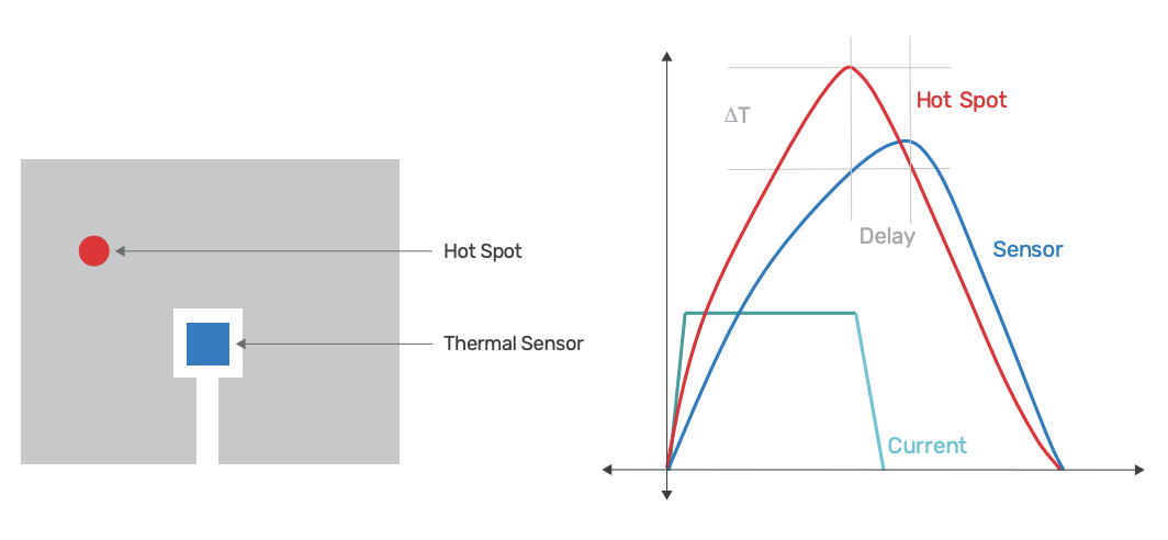
During the normal operating lifetime, one of the major sources of failures is thermal overstress. Devices that drive actuators operate at high power, which further increases the temperature of the device (Figure 2). The stress of operating at high temperature can cause devices that have been designed for a long operating lifetime to fail sooner. The Legato Reliability Solution’s electrothermal simulation provides two electrothermal simulation engines: static and dynamic. The static engine analyzes the average temperature rise of a die during normal operation. The dynamic engine analyzes the warm-up and cool-down temperature transients during normal operation. A built-in thermal extractor creates the thermal model of the die that is used in thermal simulation to simulate the temperature rise due to device power dissipation. Electrothermal simulation is based on the Spectre APS transient analysis, allowing designers to easily assess the effect of on-die temperature variation on circuit performance.

Figure 2: Sensor placement in relation to hot spot and time elapsed of peak temperature versus actual temperature

Advanced Aging Analysis

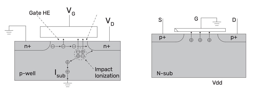
Device wear-out results in end-of-life failures. To extend device lifetime, designers need to accurately predict the effect of stress on a device lifetime. Until now, designers had to account for each source of device degradation in isolation. They use reliability analysis to estimate device in one analysis due to electrical stress, then de-rate the lifetime based on estimated die temperature and the effect of process variation. Advanced aging analysis unifies these analyses, so designers can include all the sources of device degradation. In addition, a new device aging model based on the most recent research in device physics provides better prediction of device degradation due to hot carrier injection (HCI) (Figure 3) and bias temperature instability (BTI). The Legato Reliability Solution’s advanced aging analysis provides designers the ability to better predict the operating lifetime of their designs.

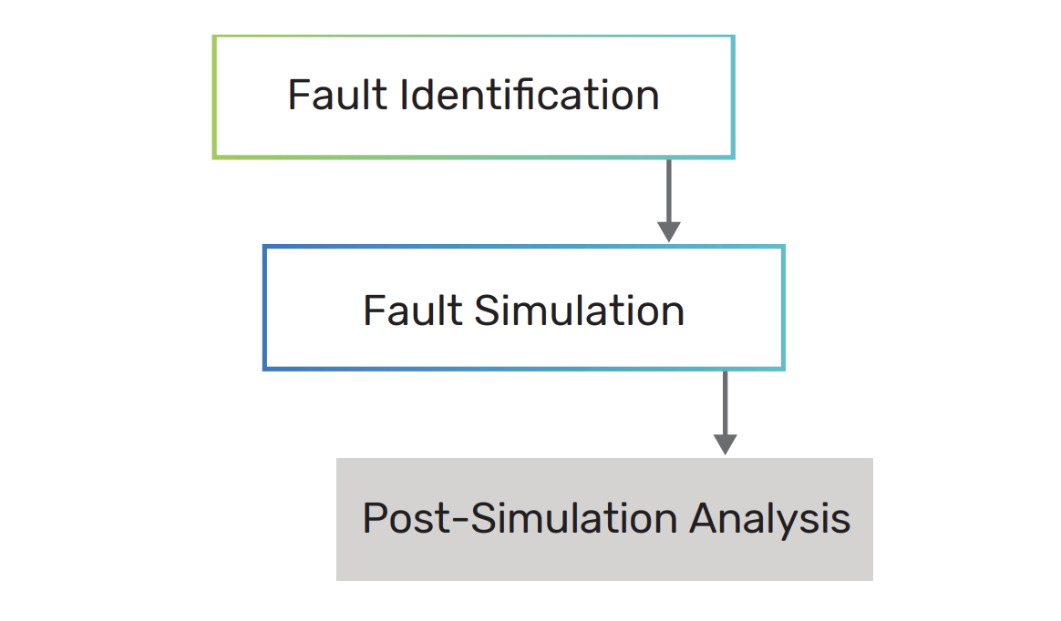
 

Figure 3: Hot carrier injection (HCI)

Cadence Services and Support

  • Cadence application engineers can answer your technical questions by telephone, email, or internet—they can also provide technical assistance and custom training. 
  • Cadence-certified instructors teach more than 70 courses and bring their real-world experience into the classroom. 
  • More than 25 Internet Learning Series (iLS) online courses allow you the flexibility of training at your own computer via the internet. 
  • Cadence Online Support gives you 24x7 online access to a knowledge base of the latest solutions, technical documentation, software downloads, and more.
  • For more information, please visit support and training.