Datasheet
ESD Cross Domain Checker
VCAD Productivity Package for Virtuoso
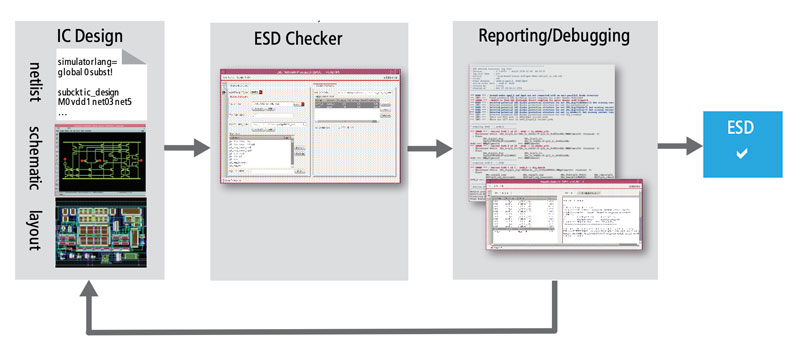
The verification of electrostatic discharge (ESD) protection in today’s IC designs is challenging and, because it is mostly done manually, it is also error prone. The Cadence VCAD Services ESD Cross Domain Checker addresses the verification of sufficient ESD protection of devices on power domain crossing signals, which is often overlooked but increasingly important for sub100nm processes on large systems-on-chip (SoCs). The solution also applies checks for basic ESD protection.
Overview
Overview
The ESD checker operates on CDL or SPICE netlists and schematics or extracted layouts (av_extracted views).
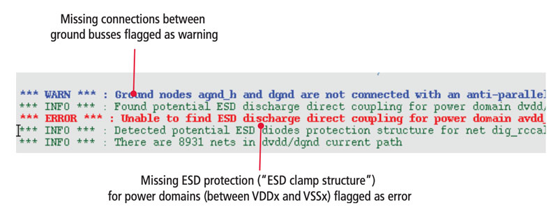
The checker identifies and flags devices on domain crossing signals. The solution also checks designs to verify ground coupling and the existence of ESD clamping on all power domains.
For identified critical elements, the tool generates corresponding ESD sub-networks as Cadence Spectre netlists to ease simulations.
The ESD Cross Domain Checker relies on the following Cadence tools:
-
 Assura Layout vs. Schematic Verifier (LVS) netlist processing
 - Virtuoso Layout and Schematic Editor
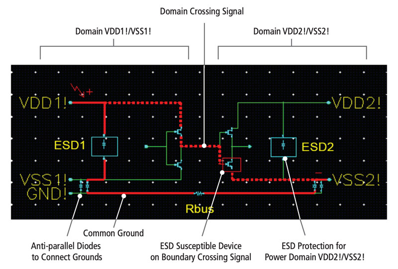
Finding ESD Susceptible Devices on Boundary Crossings
- ESD event can occur between different supply pads, e.g. VDD1! to VSS2!
- The pulse will discharge over the designated discharge path: VDD1!-ESD1-VSS1!-diodes-GND!Rbus-diodes-VSS2!
- The current pulse (amps) through the discharge path will build up a voltage drop, which can become significant, depending on Rbus
- This voltage drop can now threaten devices connected to a signal that crosses power domain boundaries
- Transistor gates with ultra-thin gate oxides (sub-100nm technology nodes) are particularly susceptible; a voltage of some volts may destroy them
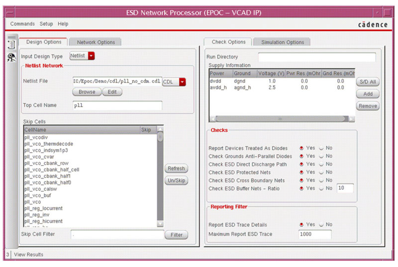
The Tool Interface
Design options
- The Input Design Type - Netlist (file and top cell) or DFII (library/cell/view)
- A Device Configuration File needs to be set up once for the PDK, for the partitioning of the design into power domains (network options)
- Skip cells allow you to omit (core) blocks of the design to speed up the processing. Select cells carefully.
Check options
- The Run Directory for data and log files of the run
- In the Supply Information field, you can enter the design’s power domains and check them against each other for ESD susceptible boundary elements
- The Checks field allows you to select from the list of implemented checks
- Control details and the length of the report via the Reporting Filter
The Implemented Checks
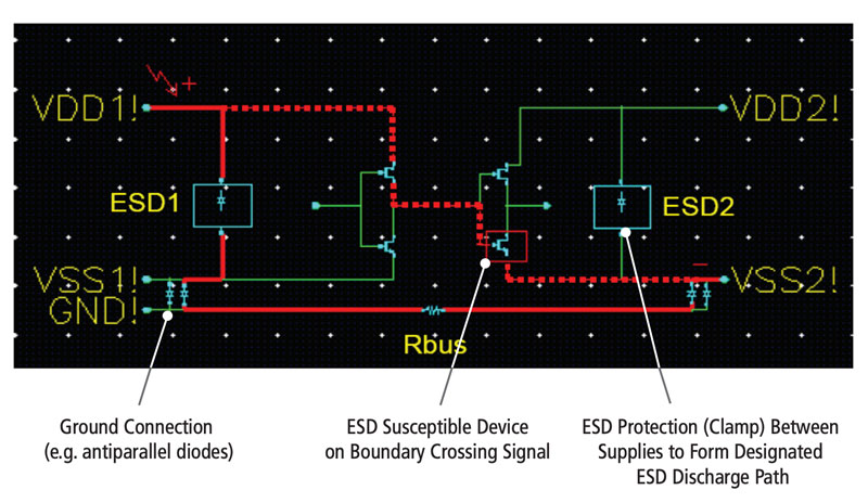
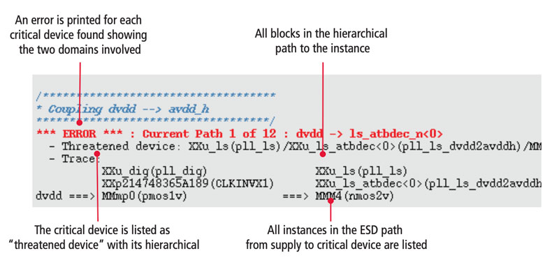
The main functionality of the tool is to report for ESD susceptible devices alongside associated ESD discharge paths. Figure 4 shows an ESD susceptible device and correctly placed ESD clamps and ground connection.
Results Reporting
After the run has finished, a report comes up when any detection of type error or warning in the design has been made, showing the results as INFO, WARN, and ERROR messages.
ESD Simulations of Critical Sub Networks
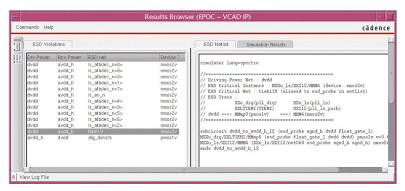
The ESD Checker helps prepare ESD simulations. It extracts the critical path from supply to supply (shown in Figure 2 as a dotted line) as a Spectre netlist. This netlist can now be incorporated in a testbench and simulated to see the effect of an ESD pulse on the transistor at the boundary crossing signal to further evaluate whether a dedicated protection on this signal is needed.
By activating the menu item Commands->View Results from the tool interface, you can bring up the Results Browser (Figure 7). It lists all critical devices found - under the tab ESD Violations. Selecting a violation displays the relevant netlist in the right half under tab, ESD Netlist.
VCAD Productivity Packages
VCAD Productivity Packages are a set of pre-packaged generic core solutions that increase design system productivity. Productivity Packages are available within services contracts, which include the package integration and maintenance of the customized solution. Cadence VCAD services targets the development, implementation, and ongoing improvement and maintenance of productive design systems to ensure short time to market and silicon success.
The EPOC tool is delivered by VCAD Services. For more information please contact:
Louis Thiam
Tel.: +49 89 4563 1957
E-mail: thiam@cadence.com
Steffen Lorenz
Tel.: +49 89 4563 1936
E-mail: lorenz@cadence.com
Cadence Design Systems GmbH
Mozartstrasse 2 85622 Feldkirchen
Germany