Datasheet
EMX Planar 3D Solver
The gold standard in chip-level electromagnetic modeling
Overview
Overview
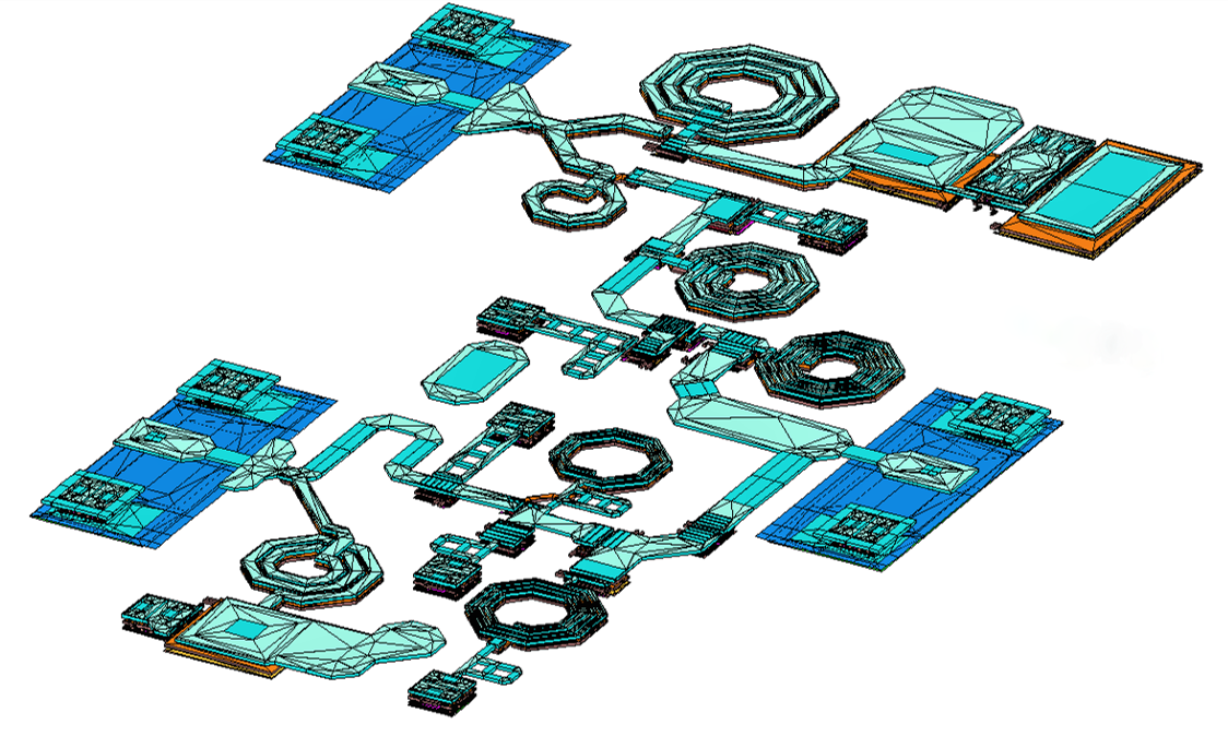
The Cadence EMX Planar 3D Solver is an electromagnetic (EM) simulator for high-frequency and high-speed integrated circuits. It allows designers to accurately and efficiently simulate large circuit blocks, characterize the behavior of passive components, and analyze on-chip EM parasitics. The solver’s unique emphasis is on design flow automation, coupled with uncompromised speed and accuracy. The EMX Solver has been benchmarked to be more than an order of magnitude faster than other electromagnetic solvers in the industry. It is built on a philosophy of maximal automation, with industry-standard input and output formats and automated handling of modern IC layout features. EMX Planar Solver shortens design cycles and brings better products to market with less risk.
EMX Planar 3D Solver has been the semiconductor industry’s preferred EM simulator for over 15 years. It has been used in thousands of successful tapeouts across all different foundries and process nodes down to 2nm, and it has been extensively characterized versus silicon measurements for the accuracy of the EM models it produces.
The EMX Solver has a significant speed advantage over other commercial EM simulators. The modeling engine is based on the Fast Multipole Method (FMM) that solves the matrices resulting from solving Maxwell’s equations. Additionally, it takes advantage of any symmetries in the geometry, giving designers the benefit of not having to recalculate identical interactions between similar meshes.
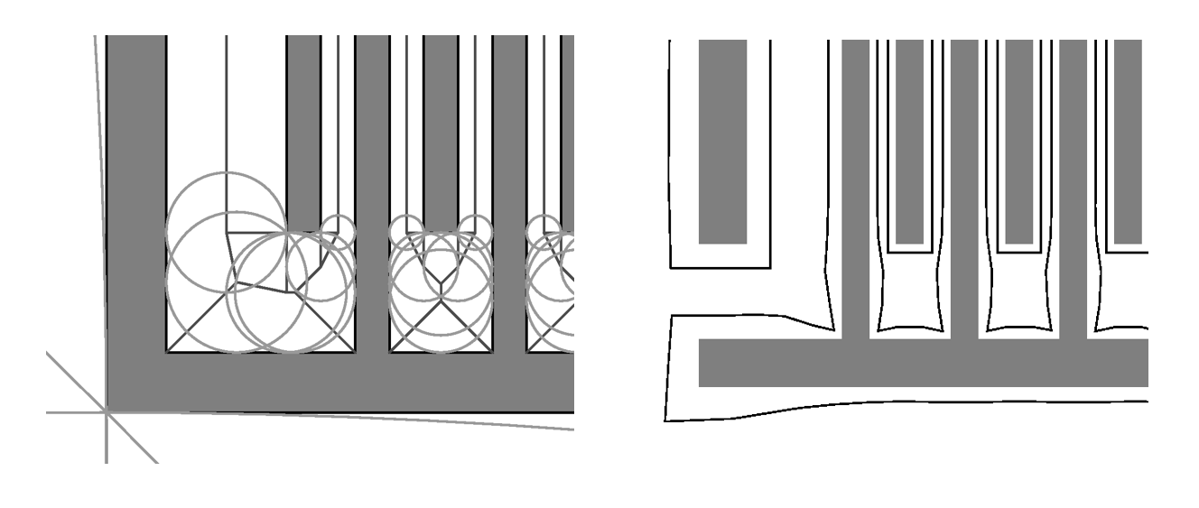
EMX Planar 3D Solver can accurately model advanced-node process fabrication effects, including width- and spacing-dependent effects and double patterning (Figure 2), as these are described in a process tech file, and producing very accurate models for the lower-nm nodes.
The EMX Solver is seamlessly integrated into Cadence’s custom analog design flow and with all Virtuoso releases, as well as with the analog design environment and Spectre RF. An integral part of the Virtuoso RF design flow, the EMX Solver integrates with the Quantus Extraction Solution through the Smart View feature, enabling “EM-aware” parasitic extraction and signoff.
Features
Hybrid Volume and Surface Formulation
Cross-fabric design applications require a smarter, more efficient way of solving from EM software. The EMX Planar 3D Solver supports a hybrid formulation where thick conductor layers can now be solved using a new surface formulation. In addition, support continues for the existing volume formulation for thinner metal layers.
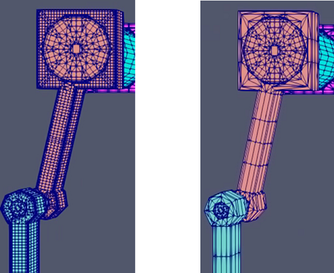
Surface formulation allows users to specify thicker conductor layers, for example, interposers and package layers, and have the EMX Solver discretize and solve these layers more efficiently by applying a surface mesh (Figure 4). Skin effect is the predominant effect at higher frequencies, and the surface meshing option results in significantly faster modeling times, up to 10X for the larger test cases, and up to 70% reduction in memory requirements, without any penalty in the accuracy of the produced models.
Adjustable Dynamic Range for Low Coupling (k) Applications
The EMX Solver supports various levels of dynamic range and a noise floor down to -120dB. Tighter modeling engine options ensure accuracy and passivity at very low levels to capture weak coupling effects for isolation studies and lower signal-level designs.
Process Parallelization
The EMX modeling engine is fully parallelizable, solving for frequency and ports. The software supports MPI, a standardized message-passing system for running parallel applications on networks of computers. Ideal for CPU-based compute farms, MPI brings significant benefits to simulation time when the number of ports exceeds 100. The EMX Solver machine parallelism is recommended for use when the structure to be solved has both a high mesh complexity and a high port count.
The recommended memory option performs computations at the beginning of the solver run to size the problem and set an optimal memory limit. The user is notified early in the run if either the machine’s memory or the user-specified memory limit is below the computed memory limit and could possibly constrain the speed of the solver run. The scheduling of solving complex networks is more efficient and avoids over-reserve memory. Annoying, time-consuming crashes due to the unavailability of the required computing resources are also avoided.
Flow Integration for EM-Aware Parasitic Extraction and Signoff
Cadence’s Virtuoso RF design flow with Smart View offers unique integration with the EMX Solver for modeling EM-sensitive content using the Quantus solution for layout parasitic extraction. Tightly integrated within the Virtuoso Studio platform, the EMX Solver creates EM models per net and per metal layer based on a user-defined selection from either the schematic or the layout editor. Results from the Quantus and EMX solutions are automatically stitched into the resulting netlist and extracted view, saving the designers from a very time-consuming and error-prone process, especially in designs with a large count of layout pins. Ideal for both analysis and EM signoff, the EMX Planar 3D Solver helps designers de-risk their designs from EM coupling.
Run Mode and Save/Load Processed Layout/Mesh Files
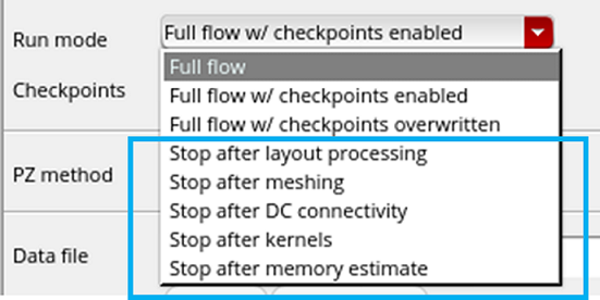
A new “run mode” feature has been introduced to allow an EMX Solver job to stop at various stages of the simulation before a full flow is finished (Figure 5). This gives users certain information, such as DC connectivity results, mesh size, or recommended memory, without waiting for the full simulation to end or manually terminating the remaining EMX Solver run.
An EMX Solver simulation can be stopped at various stages, i.e., after layout processing, meshing, etc. The save/load files feature allows users to save several intermediate files generated during an EMX Solver run and to use the saved files in later simulations (when applicable) to speed up the simulation. This feature is helpful if the users know that they will obtain certain information (such as mesh size/recommended memory) from an initial run and then kick off a second run based on their learning from the first run while saving some simulation time by re-using saved intermediate files from the first run.
Integration with Virtuoso EM Assistant Enables Cross-Fabric EM Analysis
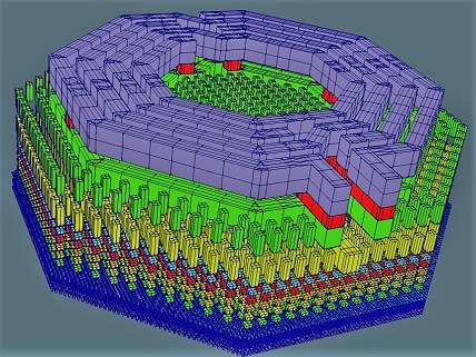
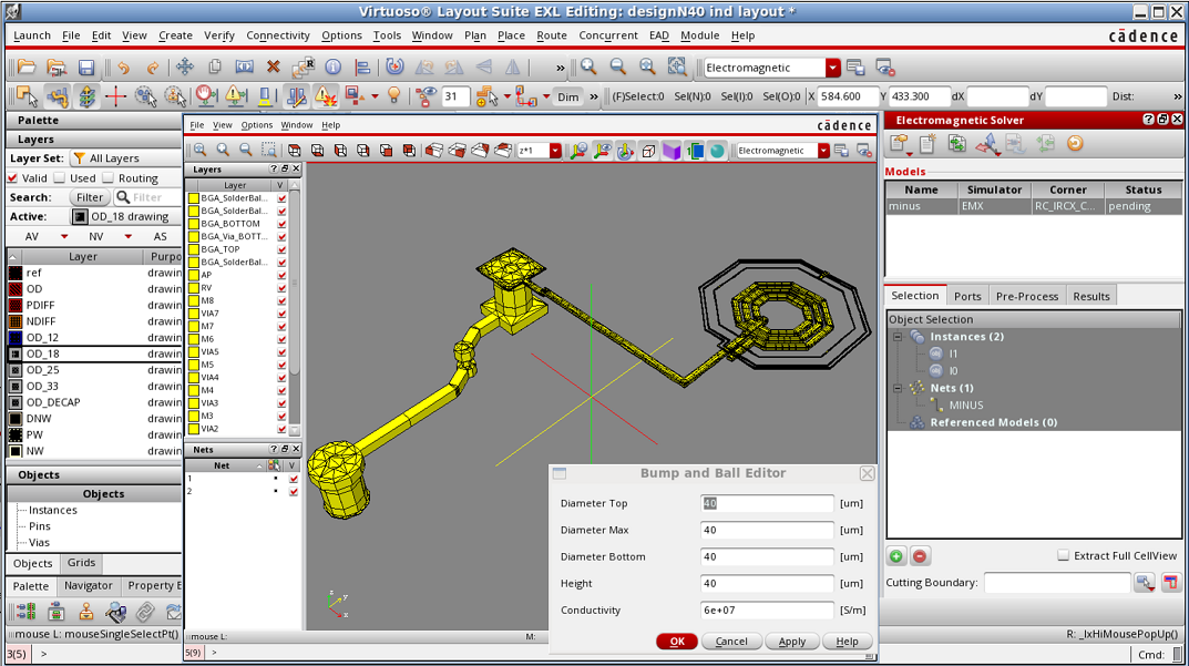
Integrating the EMX Solver with the EM assistant functionality of Virtuoso Studio allows true chip+package EM co-simulation in a unified design environment (Figure 6). The designer can import Allegro databases of package designs into Virtuoso Studio and define nets from the package layout as well as from the chip layout, then co-simulate using the EMX Solver, taking into account capacitive and magnetic coupling interactions between IC and package.
The EMX Solver can automatically merge chip and package tech files and selectively apply volumetric and surface meshing to optimize the efficiency of the modeling process. The Virtuoso RF flow then takes over and automatically connects the N-port to the schematic hierarchy, saving the users from the time-consuming and error-prone process of manually stitching together multi-port symbols.
