Datasheet
Cadence Sigrity PowerSI
Frequency-domain power- and signal-integrity analysis
The Cadence Sigrity PowerSI environment provides fast and accurate full-wave electrical analysis of leading-edge IC packages and PCBs to overcome increasingly challenging design issues such as simultaneous switching noise (SSN), signal coupling, problematic decoupling capacitor implementations, and design regions that are under or over target voltage levels. The Sigrity PowerSI approach can be used before layout to develop power integrity (PI) and signal integrity (SI) guidelines as well as post-layout to verify performance and improve designs without a physical prototype. PowerSI capabilities can be readily used in popular PCB, IC package, and system-in-package (SiP) design flows.
Overview
Benefits
Advanced Analysis Techniques
Fast and accurate
PowerSI efficient electromagnetic analysis techniques are ideal for modeling entire PCBs or IC packages with full-wave accuracy. PowerSI speed stems from unique patented methodologies that allow for autoadaptive numerical meshes, enabling accurate modeling for complex structures such as cuts and slots in planes, multiple power and ground layers, and any number of vias and traces. PowerSI intelligent multi-processor support distributes simulations for the fastest possible throughput. With an optional high-performance computing license, simulations can be distributed across multiple machines to further enhance throughput. With the PowerSI approach, designers can fully analyze and strategically tune their designs to achieve performance and schedule objectives.
Comprehensive analysis
Unlike traditional SI tools that treat power and ground planes as ideal with fixed voltages, the PowerSI approach fully considers all signal and plane effects simultaneously. This is achieved in an environment that provides a high degree of automation. With the PowerSI approach, there is no need to segment designs before simulation. This eliminates cumbersome design preparation while also offering greater accuracy than evaluating a system a few components at a time, as required by approaches relying on traditional 3D analysis.
Flexible Workflow
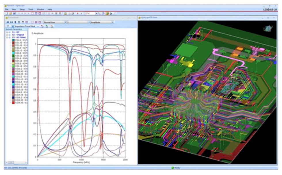
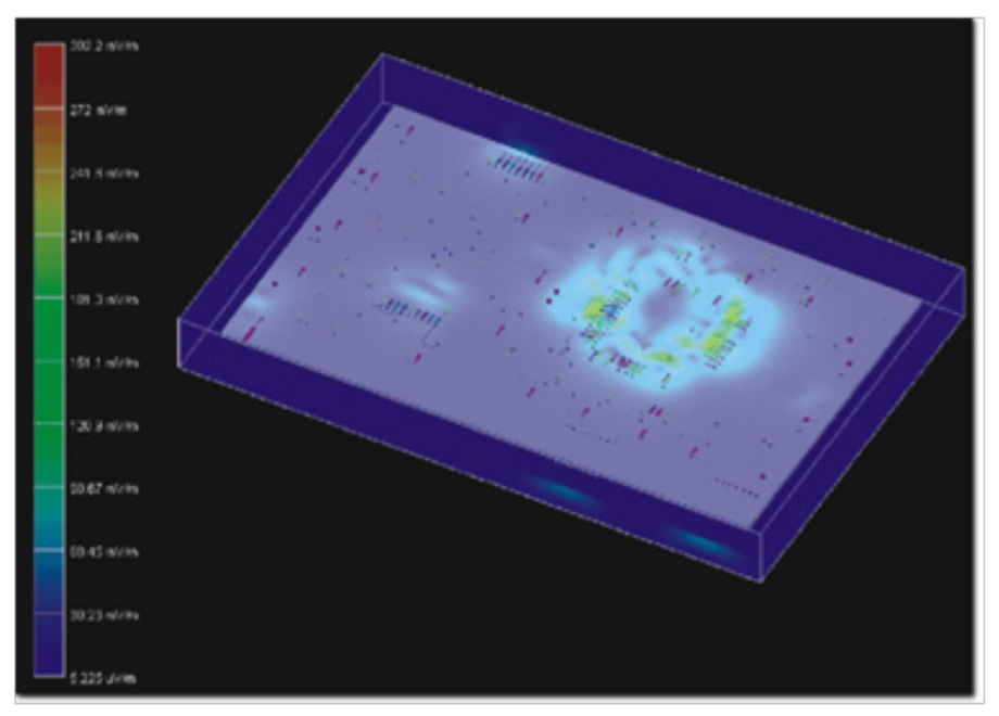
In Extraction mode, the PowerSI environment provides a convenient way to extract S, Z, and Y parameters of userselected ports. With simulations in Spatial mode, the PowerSI approach facilitates AC analysis to assess voltage distribution across ground planes. Users can flexibly control observation locations to focus on areas of interest such as voltage levels between plane pairs and performance for specific frequency ranges. A variety of 2D and 3D visualization options enables rapid results assessment. PowerSI capabilities incorporate a task-focused workflow that can be customized to provide step-bystep guidance tuned for frequent analysis tasks and to establish defaults to guide new users.
Proven Capability
Designs today are called on to create quality products at the lowest possible cost. The PowerSI environment enables early issue detection and streamlines resolution. Early visibility into potential EMI issues complements PI and SI capabilities. Near- and far-field radiation is displayed along with 3D geometry information. With the PowerSI approach, designers can fully analyze and strategically tune their designs to increase market advantage, which is why the Sigrity advanced SI and PI solutions are used by nearly every major electronics company in the world.


