Brochure
TX Controller IP for MIPI DSI
Overview
Overview
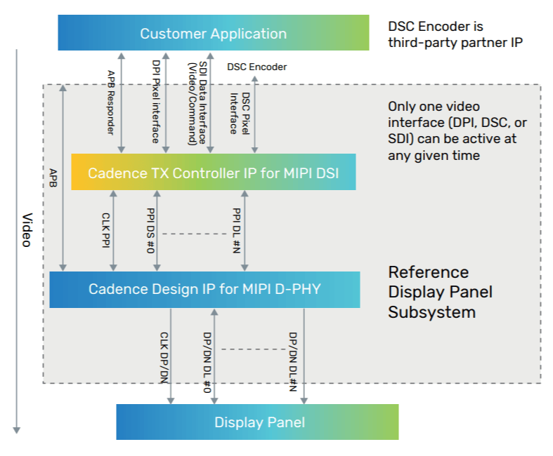
The Cadence Transmitter (TX) Controller IP for MIPI DSI is compliant with the MIPI Alliance Specification for Display Serial Interface (DSI) version 1.3.1. The TX Controller IP for DSI provides the interface from a host device graphics controller to one or more display modules and includes an arbitration layer for arbitrating among the various data and command streams, a DSI protocol layer for protocol functions, a lane management layer (LML) to distribute the DSI data stream across the active D-PHY lane modules, and an external register interface for configuration of the controller IP and status/error reporting.
The TX Controller IP for DSI is architected to rapidly and easily integrate into any system-on-chip (SoC), and to connect seamlessly to Cadence or third-party PPI-compliant D-PHY lane modules.
The TX Controller IP for DSI provides a cost-effective, low-power solution for demanding applications. It offers SoC integrators the advanced capabilities and support that not only meet but exceed the requirements of high-performance designs and implementations.
All Cadence IP for MIPI is silicon proven and has been extensively validated with multiple hardware platforms.
Product Details
The TX Controller IP for DSI supports the MIPI DSI protocol for both video and command displays. The DSI link can be switched between command mode and video mode without resetting the Transmitter IP.
Benefits
-
 Flexible interface options, including support for DPI, SDI, and DSC
 - Automotive variant available, with safety manual
- Flexible Command mode support via APB interface or SDI
Key Features
- Compliant with MIPI DSI v1.3.1
- Supports both Command Mode and Video Mode
- Supports bi-directional low-power data transmission (LPDT)
- Cadence Serial Display Interface (SDI), MIPI Display Pixel Interface (DPI), and Display Compression (DSC) input interface options
- Connects to MIPI D-PHY lane modules through PPI (up to 4 data lanes)
- Provides protocol error detection
- Programmable test video generator for integration debug and test
- 32-bit Arm AMBA 3 Advanced Peripheral Bus (APB) responder interface for register access
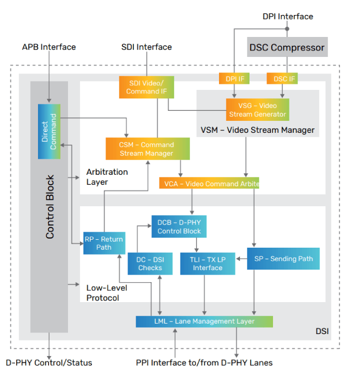
Arbitration Layer
The Arbitration Layer takes pixel data input from the selected video interface, resynchronizing where necessary, and command data from either the SDI or the Direct Command buffer in the Control Block and arbitrates between the two sources based on the programmable Controller configuration. Selected data streams are then passed to the DSI protocol functions. A Test Video Generator is also provided in this module, when enabled and selected.
Low-Level Protocol Layer
The low-level protocol layer accepts the data stream from the arbitration layer, creates packet headers, calculates payload CRC values, and adds DSI-specific control packets to create the DSI packet stream. It also provides D-PHY lane module control during start-up. The low-level protocol layer also receives data from the remote display peripheral in the bi-directional LPDT mode, and applies error detection and correction before passing packets to the control-block receive buffer, from which it can be accessed by the application processor.
Control Block
The control block contains the configuration, status, and error reporting registers used by the TX Controller IP for DSI. It supports a 32-bit APB responder interface for connecting the controller IP to an application processor.
Related Products
- Cadence Design IP for MIPI D-PHY
- Cadence TX Controller IP for MIPI CSI-2SM
- Cadence RX Controller IP for MIPI CSI-2
Deliverables
- Unencrypted, synthesizable Verilog HDL
- Cadence Genus Synthesis Solution scripts
- Documentation—Integration and User Guide, Release Notes
- Demonstration testbench, using System Verilog and Cadence Verification IP (VIP)
- Software Driver
For more information, visit Design IP.