Brochure
TX Controller IP for MIPI CSI-2 v2.1
Overview
Overview
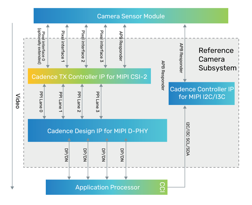
The Cadence Transmitter (TX) Controller IP for MIPI Camera Serial Interface 2 (CSI-2SM) is responsible for handling and encoding image sensor data (in multiple RGB, YUV, and RAW formats), as well as user-defined data formats, and converting these into CSI-2-compliant packets for transmission over a MIPI D-PHYSM link. The TX Controller IP for CSI-2 supports up to four independent pixel streams and can perform Virtual Channel and Data Type interleaving before transmission. Developed by experienced teams with industry-leading domain expertise and extensively validated with multiple hardware platforms, the TX Controller IP for CSI-2 is engineered to quickly and easily integrate into any systemon-chip (SoC) design, and to connect seamlessly to a Cadence or third-party D-PHY via standard PHY-Protocol Interface (PPI).
The TX Controller IP for CSI-2 is part of the comprehensive Cadence Design IP portfolio comprised of interface, memory, analog, and system and peripheral IP
Product Details
The TX Controller IP for CSI-2 is compliant with MIPI Alliance Specification for CSI-2 version 2.1. It supports all primary and secondary data formats from the specification. Support for data scrambling and LRTE EPD Options 1 and 2 are both configurable.
The TX Controller IP for CSI-2 is an all-digital design consisting of an external register interface for configuration of the transmitter IP, a Protocol Module for CSI-2 protocol functions with a data packer to convert the pixel stream input into the correct data format for transmission, arbitration for sequencing up to four pixel streams, and a TX Lane Control module for dynamic control of the PPI D-PHY interface.
Protocol Module
The CSI-2 Protocol Module handles the CSI-2 protocol stream coming from the pixel stream interfaces and monitors traffic on the interfaces. It also performs error checking, interrupt generation, and CRC code generation to ensure data integrity.
The CSI-2 Protocol Module also monitors the CSI-2 protocol stream for start-of-frame (SOF), end-of-frame (EOF), and truncated CSI-2 frames. This module provides the asynchronous FIFO between the pixel stream interface and the D-PHY byte transmission.
RX Compatibility Mode allows direct connection from the pixel interface output of the CSI-2 RX Controller IP to the CSI-2 TX Controller meaning Virtual Channel interleaving can be supported on a single stream.
CSI-2 Packer
The CSI-2 packer formats data from RAW Bayer, RGB, and YUV packed data formats into the CSI-2 format for transmission on the PPI D-PHY interface.
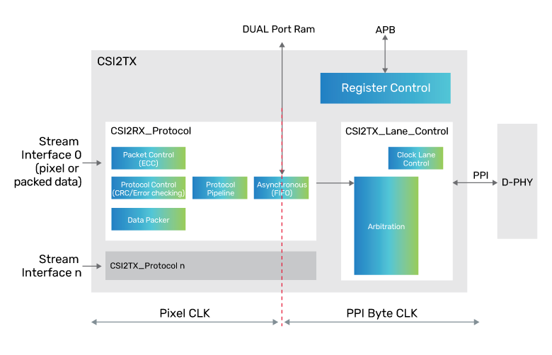
CSI-2 Arbitration
The CSI-2 arbitration allows Virtual Channel and Data Type interleaving by arbitrating between pixel streams to data lanes.
TX Lane Control Module
The TX Lane Control Module provides conversion of data packets to bytes for transmission via the D-PHY, via the PPI. The Lane Control Module also drives the signals which control transition of the D-PHY in and out of High-Speed, ULPS, and LRTE-Idle states. Some additional D-PHY control outputs allow resets to be applied and polarity inversion to be enabled (if supported by the D-PHY).
Benefits
-
 Highly configurable IP core is area optimized for each application
 - Complete solution—both host and peripheral IP available
- Multi-stream pixel interface support
- Automotive variant with Safety Manual
Key Features
- Compliant with MIPI CSI-2 v2.1 Specification
- Support for MIPI D-PHY v2.1 specification, with 8-bit PPI data width and links with 1, 2, or 4 data lanes
- Provides up to 4 independent stream input interfaces, with a highly configurable range of options, including multiple pixel modes, various buffering modes, packed data mode, and Data Type interleaving
- Optional extensions for loopback support on stream 0, for connection to Cadence Receiver Controller IP for CSI-2 (“RX Compatibility” mode
- RTE – Efficient Packet Delimiter support (Option 1 and 2)
- 32-bit Arm AMBA APB Responder programming interface
- Programmable Data Type and Word Count settings, with either 8 or 16 options selectable on a packet-bypacket basis
- Support for external RAM/register or internal register-based stream buffer
- Support for all primary and secondary data formats
- Supports ULPS on all data lanes and clock lane
Related Products
- Cadence Design IP for MIPI D-PHY
- Cadence RX Controller IP for MIPI CSI-2
- Cadence Display Controller IP for MIPI DSISM
- Cadence Initiator Controller for MIPI I3CSM
- Cadence Responder Controller for MIPI I3C
Deliverables
- Unencrypted, synthesizable Verilog HDL
- Cadence Genus Synthesis Solution scripts
- Documentation—Integration and User Guide, Release Notes
- Demonstration testbench with integrated Cadence Verification IP (VIP)
- Software Driver
For more information, visit designip