Brochure
Think Beyond the Chip

Cadence is certainly well-known for our design tools for integrated circuit (IC) design. I run the custom and analog IC part of that, built around our Virtuoso custom IC design platform. But that’s not the focus of this paper. Instead, I want to encourage everyone to “think beyond the chip”. In addition to custom IC layout, I also run our semiconductor packaging and printed circuit board (PCB) design tools built around our Allegro environment, our radio frequency (RF) design tools, and multi-physics system analysis.
Overview
Beyond the Chip
There are multiple big trends “beyond the chip”:
One thing all of these domains depend on is Cadence’s deep competence in computational software, especially scaling analysis into the cloud to produce speedups of an order of magnitude or more.
Multi-Chip(let)
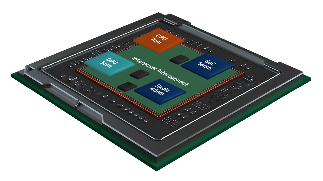
With Moore’s Law slowing, it is increasingly attractive to construct advanced systems out of chip(let)s from multiple processes. Some designs require the performance and density of the most advanced nodes, but that is generally only effective for digital designs.
Analog does not scale easily, and FinFETs with quantized transistor sizes are even less attractive. The capacitance of the transistors is also too high for on-chip RF design to be effective.
Cadence has been working in advanced IC packaging for a long time. In fact, virtually every BGA/LGA package built in the past 25 years was designed with our tools. This puts us in a great position to extend our leadership in this area into the next generation of 2.5D-/3D-IC heterogeneously integrated packages, but these designs will increasingly be designed in Cadence’s Innovus Implementation System for digital ICs.
Cadence has a product called the Integrity System Planner that is used for managing and optimizing chip(let)s, packages, and boards at the system level in a single canvas. But beneath that, all three of our major design environments can support designing all the chip(let)s, the package, and extending into the PCB. The Allegro environment is ideal for things that are PCB-like (high-density RDL fan-out wafer-level packages), the Virtuoso environment for designs that are more silicon- centric, and Innovus Implementation for any high-capacity digital-centric design.
While we are addressing thermal/power/signal tradeoffs, we must take care to ensure EM interference doesn’t also become a problem.
EM Analysis
About 30 years ago, the ball grid array (BGA) was invented, which provided the ideal platform for flip-chip designs with improved performance and better power delivery. It also ushered-in a switch from using clocked parallel interfaces with lots of pins to using very fast serial interfaces, driven by serializer-deserializer (SerDes) blocks.
The highest speed interfaces today are called 112G (112 Gigabits per second), which is extraordinarily fast. “We used to call these frequencies microwave,” an engineer told me recently. That means that their electromagnetic (EM) analysis is complicated. At these frequencies, every little bit of conductor can affect signal integrity. Last year, Cadence announced the Clarity 3D Solver, built from scratch to handle these high-performance designs and to limitlessly scale with the cloud.
Another complication is thermal analysis, which is required to ensure heat can be adequately dissipated to ensure reliability (e.g., what is an appropriate heatsink size). However, power and signal integrity are affected by temperature, so these must be taken into account simultaneously. While we are addressing thermal/power/signal tradeoffs, we must take care to ensure EM interference (EMI) doesn’t also become a problem.
More recently, we announced the Clarity 3D Transient Solver to address large-scale finite difference time domain (FDTD) analysis. For example, the traditional way to check for EM compliance (EMC) is to put the device in an anechoic chamber with an antenna ~10 meters away. This is expensive, especially if the test fails and a redesign is required. The Clarity 3D Transient Solver can utilize cloud servers to analyze the entire system for EMC/EMI, reducing re-spins and accelerating time to market. A final anechoic test may still be required, but first-time success is much more likely.
Radios
Radios are everywhere. 5G is a big driver, but from a radio point of view, 5G consists of two very different technologies. In the low- and medium-frequency bands, the so-called sub-6GHz spectrum, there is one type of radio. A higher frequency band is mmWave, at ~25GHz and above, which requires a completely different type of radio and different antennas.
All generations of mobile communications, to some extent, use the increasing computational power of silicon to make better use of radio bandwidth (a truly limited resource). LTE broadband communication introduced MIMO (multiple-input/multiple-output) where the radio channel may involve multiple antennas. 5G introduces beam steering to direct the radio signal at the receiving antenna, thereby avoiding broadcasting in the “wrong” direction.
At the start of 2020, Cadence acquired National Instrument’s AWR subsidiary and its popular AWR Microwave Office design and analysis suite. We also acquired Integrand Software and its gold-standard EMX Planar 3D Solver, which is primarily used to analyze on-chip RF passives. Together with our Virtuoso RF platform and Spectre RF Option, the integration of all these products — along with the Clarity solvers and Celsius Thermal Solver — will provide the industry with a next-generation, comprehensive RF design solution.
Summary
Today, Cadence is working with semiconductor leaders to advance Moore’s Law, including the design of 2nm test circuits. Increasingly, the focus is on More than Moore: combining heterogeneous functionality in the form of chiplets (digital, analog, photonics, sensors, RF/mmWave, etc.) across ICs, packages, modules, PCBs, and entire electro-mechanical systems. To ensure success, these complex systems need to be thoughtfully planned, co-de- signed, and continuously analyzed. It is no surprise that EDA, mechanical design, and multi-physics software companies are experiencing strong growth. But this growth pales in comparison to the product complexity our customers are inventing.


