Brochure
RX Controller IP for MIPI CSI-2 v2.1
Overview
Overview
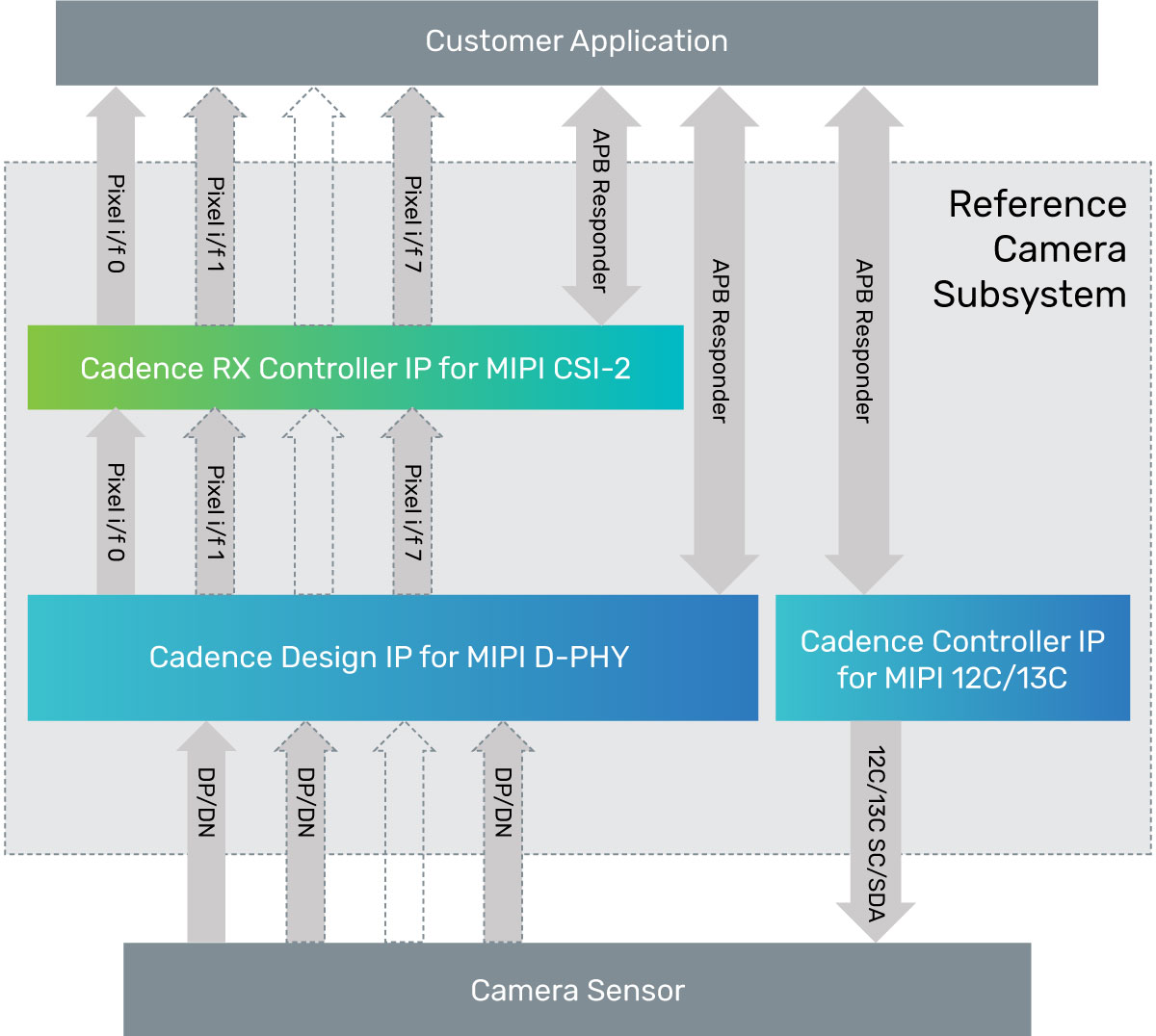
The Cadence Receiver (RX) Controller IP for MIPI Camera Serial Interface 2 (CSI-2SM) is responsible for handling and decoding CSI-2 protocol-based camera or other sensor data streams received via a MIPI D-PHYSM link and managing the forwarding or unpacking of payload data to the pixel stream interfaces. The RX Controller IP for CSI-2 allows the selection of multiple independent streams to support the control of the destination for each data packet (for example, Bayer input of ISP, RGB/YUV input of ISP, or DMA to memory).
Developed by experienced teams with industry-leading domain expertise and extensively validated with multiple hardware platforms, the RX Controller IP for CSI-2 is engineered to quickly and easily integrate into any system-on-chip (SoC) design, and to connect seamlessly to a Cadence or thirdparty D-PHY via a standard PHY-Protocol Interface (PPI).
The RX Controller IP for CSI-2 is part of the comprehensive Cadence Design IP portfolio comprised of interface, memory, analog, and system and peripheral IP.
Product Details
The RX Controller IP for CSI-2 consists of a lane management module that connects via the PHY-Protocol Interface (PPI) to a D-PHY receiver module, an external register interface for configuration of the receiver IP, a CSI-2 protocol module for protocol decode, and an optional CSI-2 stream modules for providing received CSI-2 packets from the D-PHY and providing synchronization information and pixels/packed data to the pixel stream interface. Each stream has an external memory interface that can act as a line buffer or as a short buffer to minimise latency.
Benefits
-
 Full featured and highly configurable IP core is area optimized for each application
 - Complete solution-both host and peripheral IP available
- Emulated on Palladium and validated in FPGA platforms
- Multi-stream pixel interface support
- Automotive variant with Safety Manual
Key Features
- Compliant with MIPI CSI-2 v2.1 Specification
- Provides up to 8 independent stream output interfaces, with a highly configurable range of options, including multiple pixel modes, various buffering modes, packed data mode, Data Type selection, and Virtual Channel or Data Type interleaving
- Configurable internal data path width of 32 or 64 bits to allow system clock frequency reduction
- LRTE-Efficient Packet Delimiter support (Option 1 and 2)
- Support for all primary and secondary data formats
- 32-bit Arm AMBA APB Responder programming interface
- Protocol-only support (no stream modules) for raw decode of CSI packets and error detection, providing extremely low gate count
- Support for MIPI D-PHY v2.1 specification, with 8-bit and 16-bit PPI data width and links with 1, 2, 4, or 8 data lanes
- Support for external RAM/register or internal register-based stream buffer
- Supports ULPS on all data lanes and clock lane
Lane Management Module
The RX Controller IP for CSI-2 front module receives 8 or 16 bits from each enabled D-PHY data lane via the PPI interface and packs it into the 32-bit or 64-bit datapath for transfer to the CSI-2 protocol module. The D-PHY deskew and ULPS entry/exit conditions are monitored in this module. An optional descrambling block will decode any incoming scrambled data.
Protocol Module
The RX Controller IP for CSI-2 protocol module decodes the CSI-2 protocol stream coming from the camera/sensor interfaces. It also performs error checking and correction and a cyclic redundancy check (CRC) to ensure data integrity. The CSI-2 protocol module also monitors the CSI-2 protocol stream for synchronization events.
Stream Module
The RX Controller IP for CSI-2 stream module can provide packed data or pixel data in single, dual, quad, or octal pixel per clock cycle to the system. The pixel interfaces support flow control to allow the system to stall the data stream.
The stream module formats data from CSI-2 packets into RAW Bayer, RGB, YUV, and user-defined packed data formats. Up to eight highly configurable streams are available, all of which will take the data received from the protocol module and provide data to the stream interface in packed or pixel format.
Certain data types support multiple pixels per pixel clock cycle to increase throughput. Three buffering modes are available:
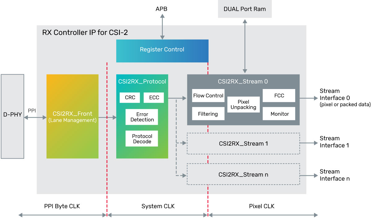
- Full-Hold full line in buffer before transfer to pixel interface
- Fill Level-A programmable watermark controls when data is transferred to the pixel interface
- Short-Data is passed to the pixel interface with low latency
Monitor and Frame Capture Control Modules
The RX Controller IP for CSI-2 provides stream channel monitors that can be configured to track and observe frames, lines, bytes, and clock cycles on individual virtual channels within each stream.
The monitors can be configured with the virtual channel and with the expected frame length to detect whenever the number of expected lines is truncated or exceeded, to count the number of lines in a frame, and to count the number of clock cycles from a start or end of a frame.
The frame capture control (FCC) function allows a specified frame number to be extracted from the incoming packet stream.
Related Products
- Cadence Design IP for MIPI D-PHY
- Cadence TX Controller IP for MIPI CSI-2
- Cadence Display Controller IP for MIPI DSI
- Cadence Initiator Controller for MIPI I3C
- Cadence Responder Controller for MIPI I3C
Deliverables
- Unencrypted, synthesizable Verilog HDL
- Cadence Genus Synthesis Solution scripts
- Documentation-Integration and User Guide, Release Notes
- Sample verification testbench with integrated Cadence Verification IP (VIP)
- Software Driver
For more information, visit Design IP.