Brochure
PHY IP for USB 2.0 for TSMC
Overview
Overview
The ubiquity of USB 2.0 in devices makes it nearly mandatory for any USB connectivity solution. The utility of USB 2.0 allows devices to have small buffers even at high data rates, supporting efficient device connection for smaller data sets in applications ranging from the mobile and consumer market, to enterprise, automotive, and internet of things (IoT).
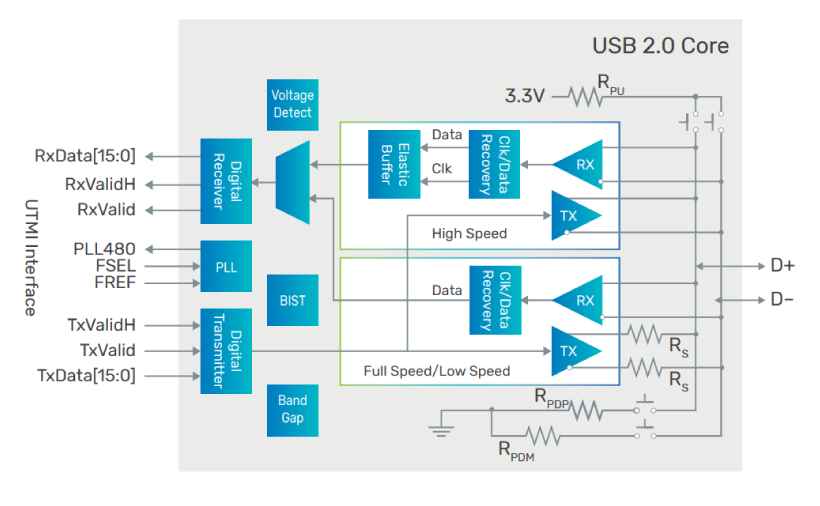
The Cadence PHY IP for USB 2.0 for TSMC is designed to the USB 2.0 specification, and operates at High Speed (480Mbps), Full Speed (12Mbps), and Low Speed (1.5Mbps). The PHY IP complies with the UTMI v1.05 specification. The PHY IP also supports the USB Battery Charging Specification, Revision 1.2.
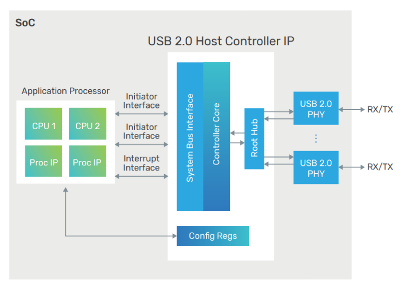
The PHY IP is architected to quickly and easily integrate into any system on chip (SoC), and to connect seamlessly to a Cadence or third-party UTMI-compliant controller. Implemented on various process technologies, the PHY IP provides a cost-effective, low-power solution for demanding applications. It offers SoC integrators the advanced capabilities and support that not only meet, but exceed the requirements of high-performance designs and implementations.
The PHY IP is silicon proven, and has been extensively validated with multiple hardware platforms. Cadence offers a comprehensive IP solution that is in volume production, and has been successfully implemented in more than 400 applications.
The PHY IP is part of the comprehensive Cadence Design IP portfolio comprised of interface, Denali memory interface, analog, and systems and peripherals IP.
Benefits
-
 Robust silicon-proven solution with USB IF certification
 - Low-power design enables power-saving applications
- Extensive test features provide improved production testing experience
Key Features
- Compliant with USB 2.0 specification and backwards compatible to USB 1.1 specifications
- Supports host, peripherals, and OTG applications
- Supports Battery Charging Specification v1.2
- Supports link power management (LPM)
- Comprehensive test features: datapath loop back, scan, BIST, bypass
- 8-bit 60MHz and 16-bit 30MHz parallel interfaces
- APB and JTAG interfaces
- Multiple reference clock supported from 9.6MHz up to 52MHz
Product Details
The PHY IP is a hard PHY macro available in various process nodes.
The PHY IP supports the USB 2.0 specification at speeds up to 480Mbps. It is designed to easily integrate with a Cadence USB controller or any third-party controller with a UTMI-compliant interface. It also supports the USB On-The-Go (OTG) supplement to provide USB host and USB device operation.
The PHY IP has flexible built-in self test (BIST) features and datapath loopback mode for improved production testing.
USB 2.0
The PHY IP is a mixed analog-digital design with High-Speed and Full-Speed analog front ends, and digital receivers and transmitters. The PHY IP includes support for suspend mode to minimize power consumption when the core is not in use. The PHY IP connects to any USB 2.0 Controller IP through an 8/16-bit unidirectional UTMI interface.
Availability
The PHY IP is available with various configurations and supports the following protocols:
| IP Name | Foundry | Geometry | Node |
|---|---|---|---|
| PHY IP for USB 2.0 for TSMC 16FFC | TSMC | 16 | FFC |
| PHP IP for USB 2.0 for TSMC 12FFC | TSMC | 12 | FFC |
| PHY IP for USB 2.0 for TSMC N7 | TSMC | 7 | FF |
Related Products
- Controller IP for USB 2.0
- Controller IP for USB 3.0
Deliverables
- Verilog behavioral modules for PHY module
- Verilog testbench with configuration files and sample tests
- Liberty timing model
- Layout abstract in LEF format
- GDSII with flat netlist for LVS
- LVS/DRC log files
- DFT views - ATPG netlist, CTL model, BSDL
- Documentation - specification and integration/user guide
For more information, visit designip.