Brochure
Integrated Design Flows for Photonics Circuits
Incorporate optical and opto-electronic effects throughout your design process
Photonics—the science and technology of generating, controlling, and detecting light—has moved into mainstream electronic designs. This is particularly true for communications hardware, where bandwidth demands are so great that only photonic ICs (PICs) offer a viable solution. Other key application areas include data centers, antenna and RF systems, bio-photonics, and environmental sensing systems.
To address the challenges of designing PICs, Cadence has teamed up with industry-leading ecosystem partners and foundries partners to develop an integrated electronic/photonic design automation (EPDA) environment.
Overview
Efficient Design Flows
Built on the industry-standard Cadence Virtuoso custom IC design platform, the EPDA environment supports monolithic (single chip carrying both traditional electronics and photonics) and hybrid (3D-IC stack with a traditional electronics chip on top of a photonics chip) approaches (Figure 1).
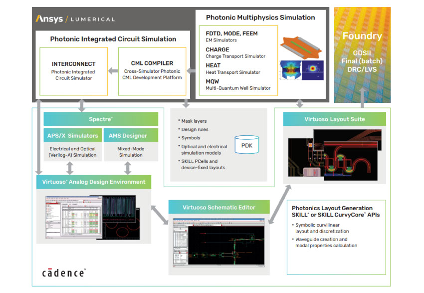
| Function | Tools |
|---|---|
| Schematic capture | Virtuoso Schematic Editor |
| Circuit simulation | Virtuoso ADE Product Suite Spectre AMS Designer Spectre APS Lumerical INTERCONNECT, a dedicated photonic IC simulation engine |
| Photonic layout implementation and parametrizable photonic cells (PCells) | Virtuoso Layout Suite |
Accelerating PIC Exploration
PIC designs come with many unique challenges over traditional electronic systems. Their curvilinear, polygon-based layouts are typically drawn by hand, which is labor intensive and time consuming. Available process design kits (PDKs) are fairly immature, with a limited amount of fixed GDS layout cells, specifications, and process rules. Error checking is quite challenging, yet layout versus schematic (LVS) and design rule checking (DRC) tools are primitive at best. Circuit modeling is also difficult without the support of a widely accepted SPICE equivalent. Often, designers end up manually drawing schematics twice when designing systems and doing the same with layouts when designing components.
The EPDA environment from Cadence and its partners addresses each of these challenges (Figure 2).
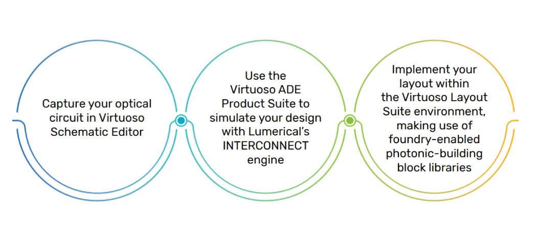
Similar to SPICE, INTERCONNECT is a dedicated time- and frequency-domain mixed-signal circuit simulation engine that has been expanded to address optical signal propagation within multimode, multi-channel components commonly found in PICs. Close integration with the Virtuoso Analog Design Environment means that you can benefit from fast PIC exploration, including yield analysis.
For PIC mask layout designs, you can tap into multiple foundries’ robust libraries of photonic PCells directly from the Virtuoso environment for interactive or scripted waveguide and component creation, including construction of complicated curvilinear shapes.
Using the EPDA environment, you can also populate your photonic PDK compact model library (CML) or create a simulation model for a custom device. The solvers in Lumerical’s DEVICE suite for photonic multiphysics simulation (FDTD, MODE, CHARGE, DGTD, FEEM, STACK) account for multi-physics optical, electrical, and thermal effects. Use Lumerical’s interoperability with the Virtuoso ADE Product Suite to perform model parameter extraction of passive and active components from the Virtuoso physical layout.
Virtuoso CurvyCore Technology
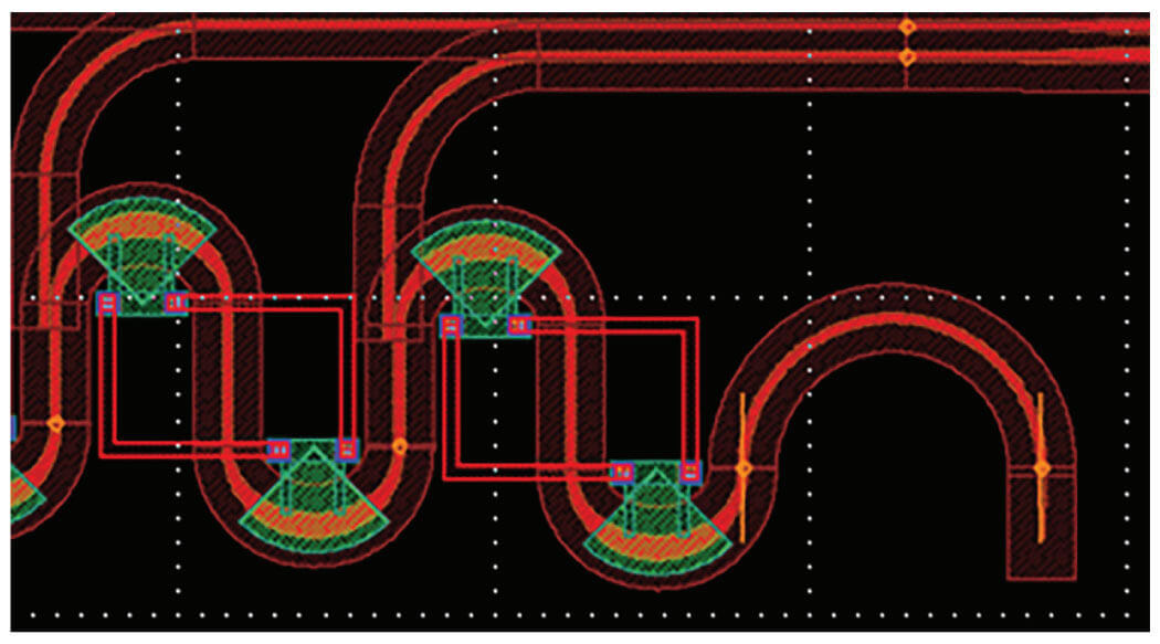
Integrated into the Virtuoso custom IC design platform, the CurvyCore infrastructure allows designers to create and edit complex curvilinear shapes common in photonics, MEMs, microfluidics, and conformal metal routing (Figure 3). Integration of the CurvyCore technology into the Virtuoso platform contributes a single design environment for developing complex multi-fabric systems.
Further Information
To learn more about Cadence photonics solutions, visit Photonics