Brochure
GDDR6 PHY IP for Samsung 7nm/14nm
Overview
Overview
Artificial intelligence (AI), high-performance computing (HPC), cryptocurrency mining, and graphics applications generate and consume large volumes of data and video and require very high memory bandwidth. The Cadence Denali DDR IP is a family of high-speed on-chip interfaces to external memories supporting these high-performance requirements with products that are optimized for each application’s needs.
The latest, the Cadence Denali PHY IP for GDDR6, is comprised of architectural improvements drawn from previous-generation DDR PHYs and Cadence’s 10G, 16G, and 25G SerDes, achieving breakthrough performance, low energy per bit, and low area relative to the bandwidth provided. This application-optimized PHY IP can achieve speeds up to 16Gbps across its full-rated range of process, voltage, and temperature, while extensions up to 20Gbps are possible with modifications. The PHY IP for provides a low bit error rate (BER) that can improve bandwidth utilization and maximum latency. The PHY IP is designed to be compatible with standard PCB materials like FR4 up to 16Gbps.
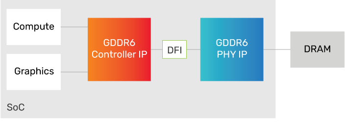
The PHY IP is developed by experienced teams with industryleading domain expertise and extensively validated with multiple hardware platforms. It is engineered to quickly and easily integrate into systems on chip (SoCs), and is verified with the Cadence Denali Controller IP for GDDR6 as part of a complete memory subsystem solution.
Benefits
-
 Derived from Cadence’s silicon-proven DDR, LPDDR, and high-speed SerDes designs
 - Highest data rates with detailed system guidelines
- Low BER even with standard PCB materials
Product Details
The PHY IP consists of a DFI interface to the memory controller, external register interface (configuration and test), PHY control block (initialization and calibration logic), PLL, and command/address and data slices, including I/Os.
The PHY IP is a high-performance SerDes-like architecture that uses SerDes design techniques to align write and read data from the I/O pads across the DFI interface to the memory controller.
Key Features
- Single configuration supports one GDDR6 device per channel (coplanar) or two GDDR6 devices per channel (clamshell)
- Memory controller interface uses DFI 5.0-like standard with extensions for GDDR6
- Internal and external datapath loop-back modes
- Per-bit DFE, CTLE, and FFE equalization
- DFI PHY Independent Mode for initialization and training
- Adaptive and continuous timing recovery
- Transmit crosstalk cancelation of immediate neighbors
- 8:1 memory:controller clock ratio for easy controller timing closure
PHY Architecture
To optimize the GDDR6 timing closure, the PHY IP is provided as a hard PHY targeting a single channel of GDDR6 supporting one coplanar or two clamshell GDDR6 devices. Several metal stacks are possible.
Data Slice and Address/Control Slices
The data slice is a 16-bit wide design that interfaces to the data and data clock connections of the DRAM. Two data slices are used to create the necessary 32-bit data width for GDDR6. If a wider interface is required, multiple instances of the GDDR6 interface should be used.
The Address and Address/Control slices interface the 11 bits to the control, command, and address connections of the DRAM. The Address and Address/Control slice is duplicated to create a point-to-point interface on command and address signals.
External Register Interface
The external register interface is a Cadence-proprietary interface to access the data slice registers.
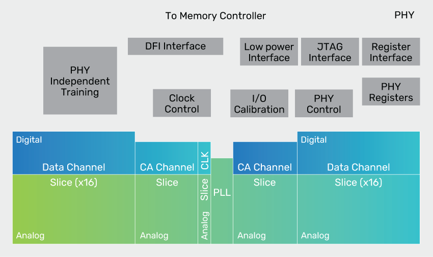
PHY Control Block
The DDR PHY IP control block provides initialization and calibration logic for training the DQS alignment for each data slice.
Availability
The DDR PHY IP is available with various configurations and supports the following protocols:
| Protocol | Speed | Process Node |
|---|---|---|
| GDDR6 | 16Gbps | Samsung 7LPP |
| GDDR6 | 16Gbps | Samsung 14LPP |
Related Products
- Denali IP for LPDDR5/4/3
- Denali IP for DDR5/4/3
- Denali IP for HBM2/HBM2E
- Denali Controller IP for GDDR6
Deliverables
- GDS II macros with abstract in LEF
- Verilog post-layout netlist
- STA scripts for use at chip or standalone PHY levels
- Liberty Timing model
- SDF for back-annotated timing verification
- Verilog models of I/O pads, and RTL for all PHY modules
- Verilog testbench with memory model, configuration files, and sample tests
- Documentation—integration and user guide, release notes
- Verification IP set up files
- Reference design for PCB and package