Brochure
Controller IP for NAND Flash
Overview
Overview
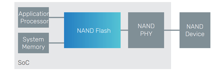
NAND Flash memory is widely used for data storage in computers and multiple consumer and enterprise applications. It is the basic building block for SSD applications, as well as USB drives, SD cards, etc. NAND Flash requires special handling and management, including error detection and correction, and the Cadence Controller IP for NAND Flash deals with those complexities, enabling our customers to create simple and quick system-on-chip (SoC) designs.
The Controller IP for NAND Flash provides the logic required to support ONFi 4.0/4.1-compliant memory in any SoC.
Supporting ONFI 4.x (excluding EZ-NAND), ONFI 3.x, ONFI 2.x., and Toggle Mode DDR-1/2 NAND Flash devices, the Controller IP for NAND Flash has many configurable features and input parameters to customize the controller for the specific needs of any application.
The Controller IP for NAND Flash is architected to quickly and easily integrate into any SoC through the industry-standard Arm AMBA 4 AXI protocol as a high-speed initiator interface and the AMBA APB and AXI-Lite protocols as register interfaces.
The Controller IP for NAND Flash is part of the comprehensive Cadence Design IP portfolio comprised of Interface, Memory, Analog, System, and Peripheral IP.
Product Details
The Controller IP for NAND Flash supports all major NAND Flash devices, with ONFI 4.1, 4, 3, 2, 1 and Toggle 2, 1 interfaces, as well as legacy asynchronous devices.
Benefits
-
 Highly-integrated IP offering—Speeds system integration and reduces design costs
 - Command and Data DMA—Reduces software overhead
- Wide support of standards—Enables system flexibility
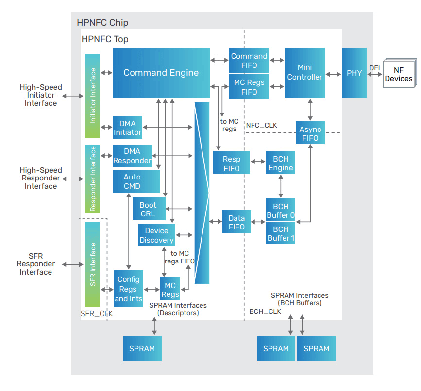
Controller Core
The controller core handles all command sequencing and flash memory device interactions, allowing intelligent hardware abstraction.
Initiator DMA Interface
The command and data DMA engines speed up data transfer between a device on the system bus and the NAND Flash memory, as well as decrease the CPU load.
Key Features
- Support for SLC, MLC, and TLC devices (in SLC mode), including for boot operation
- Advanced ECC supports different parallel factors to achieve maximum throughput
- Support for high-speed memories (up to 1200MT/s)
- Command DMA supports 32-bit or 64-bit addressing
- Support for all flash memory vendors
- Pipelined read-ahead and write commands for enhanced read and write throughput
- Supports pages sizes from 256B to 16kB
- Silicon proven and shipping in volume
- 8-bit and 16-bit flash device support
- Support for multi-LUN modes
BCH Error Correction
The Controller IP for NAND Flash supports configurable BCH implementation. The BCH engine can be configured to support error correction up to 128 bits as well as support error correction across customer-defined sub-page sizes. The BCH mechanism can be configured to support multiple error correction strength and up to two subpage sizes.
Internal FIFO
Configurable, asynchronous FIFO is used for synchronizing clock domains within the Controller IP for NAND Flash, allowing the controller core and bus interfaces to operate independently of any connected NAND Flash devices.
Cadence NAND
Driver Cadence offers the NAND Flash Controller Software Driver, aC source code driver and testbench designed to work natively with the Controller IP for NAND Flash to offload hardware management from higher level applications.
Control Interface
The control interface provides access to the configuration and status registers in the Controller IP for NAND Flash.
Related Products
The Controller IP for NAND Flash is available with various configurations and supports the following protocols:
- ONFi4.1/4/3/2/1, Toggle 2
- ONFi 4/3/2/1, Toggle 2
- ONFi 2/1
- ONFi 1
Related Products
- Cadence Soft PHY IP for NAND Flash
- Cadence PHY IP for Storage Combo
Deliverables
- Clean, readable, synthesizable Verilog RTL
- Verilog testbench with memory model and sample tests
- Cadence Genus Synthesis Solution scripts
- Documentation—integration and user guide, release notes
- Cadence NAND Driver as an optional deliverable
For more information, visit Design IP