Brochure
Controller IP for CXL
Overview
Overview
The cloud computing revolution and proliferation of mobile devices is increasing data traffic and driving changes in data center device architecture. High-speed communication within and between servers, storage, and accelerators is necessary to support video and the growth of dataset and associated analytics, with low latency key for cache coherent systems. The Compute Express Link (CXL) is based on the PCIe Express (PCIe) 5.0 interconnect, an open industry standard interconnect offering high-bandwidth, low-latency connectivity between the host processor devices such as accelerators, memory buffers, and smart I/O devices.
The Cadence Controller IP for CXL provides the logic required to integrate an endpoint (EP) controller into any system on chip (SoC).
The Controller IP has been extensively tested using Cadence Verification IP for PCIe/CXL and is built on the underlying PCIe Controller that has been tested on the Cadence Palladium series of verification computing platforms. Cadence offers a comprehensive IP solution that is in volume production and successfully implemented in dozens of applications.
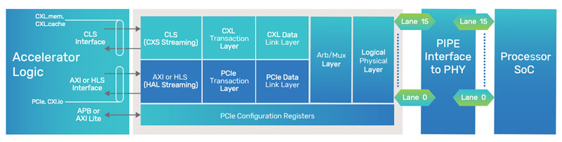
Client applications access the controller through the industry-standard Arm AMBA 5.0 AXI interface or through a native Cadence interface, the Host Adaptation Layer—Streaming (HLS).
The Controller IP is engineered to quickly and easily integrate into any CXL Cache Coherent SoC and connect seamlessly to a PIPE5.2-compliant PCIe PHY.
Compliant with CXL 2.0/1.1 and PCIe 5.0, 4.0, 3.1, 2.1, and 1.1 specifications, the Controller IP has over 100 configuration features to customize the controller to the specific needs of any computing, networking, or storage application.
Benefits
-
 Superscalar design for high throughput and low latency
 - Designed by team that is actively involved in the protocol working group
- Extensively tested with lead ecosystem drivers
Product Details
The Controller IP is designed for use in ASIC SoC devices to provide an industry-standard interface to the CXL link. It utilizes a low-latency architecture and a small silicon footprint.
Key Features
- Compliant with PCIe 5.0, 4.0, 3.1, 2.1, and 1.1 specifications
- Support for up to 4K payload size and 256 functions
- Compliant with CXL 2.0 and 1.1
- Low-latency datapath
- CXL.io, CXL.mem, and CXL.cache support for Type-1, Type-2, and Type-3 applications
- Support for latest ECNs, error counters, ECRC, and end-to-end datapath parity support
- 32b PIPE interface for 1GHz core operation
- 512bit datapath for connection to cache fabric
CXL Core
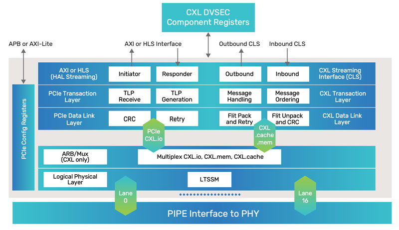
The CXL core implements the physical layer, data link layer, and transaction layer of the PCIe and CXL protocol. The physical layer provides the PIPE interface to easily connect to any PCIe-compliant PHY device, and the HLS or optional AXI interface provides connectivity to the client’s PCIe/ CXL.io interface. The CXL.mem/cache interface connects to the client logic via multiple synchronous CLS streaming interfaces. The CXL core manages the functions of the CXL protocol including flit packing and unpacking, replay buffers, flow control, and CRC check and generation.
Configuration Registers
The Controller IP implements a complete set of PCIe base configuration registers and PCIe capability registers for PCIe power management, MSI and MSI-X, PCIe, and Slot ID. In addition, the configuration registers have PCIe extended registers for advanced error reporting. An AMBA APB interface is available to access configuration and internal registers within the controller.
CXL registers are external to the Controller IP and are defined by the user. The Controller IP for CXL implements a snoop interface in order to interface to the external DVSEC registers implemented by the user.
Client Interface
The client interface is implemented to support AXI or HLS, and CXS. The client interface consists of separate initiator and responder interfaces for AXI/HLS (CXL.io) and inbound and outbound interfaces for CLS (CXL mem/cache).
CCIX Encapsulation
The Controller IP optionally supports CCIX over CXL through the lower link layer interface of the Controller, allowing it to interface to a fabric according to Arm’s CXS Issue B protocol and AES0024 and AES0026 application notes.
PIPE Interface
The PIPE family of specifications are the industry-standard PHY interface for the PCIe architecture v1.0, v2.0, v3.0, v4.0, and v5.0. In addition, the PIPE interface has an optional PCLK input for running the PIPE interface at a different clock rate than the core. CXL supports a PIPE5.2 interface in order to minimise latency.
The Controller IP is part of the comprehensive Cadence Design IP portfolio comprised of interface, memory, analog, and systems and peripherals IP.
Availability
- Controller IP for CXL 2.0/1.1 up to x16 lanes
Related Products
- PHY IP for PCIe 6.0, 5.0, 4.0, 3.1
- Controller IP for PCIe 6.0, 5.0, 4.0, 3.1
- IDE/DOE Option for PCIe and CXL
- Integrated Solution IP for PCIe/CXL
Deliverables
- Clean, readable, synthesizable RTL Verilog files
- Verification testbench example with integrated stimulus and monitors
- Comprehensive user guide
- Register descriptions
- Synthesis scripts
For more information, visit Design IP.