Brochure
16Gbps Multi-Link and Multi-Protocol PHY IP
Overview
Overview
With the large growth in data and compute demand, enterprise-level data communications, networking, and storage systems are taking center stage in many application areas. High performance and uptime, power efficiency, and small form factor are some of the key requirements for such systems, and these requirements percolate down to components and IP.
The Cadence IP for 16Gbps Multi-Link and Multi-Protocol PHY is a high-performance SerDes operating from 1.25 to 16Gbps, specifically designed for infrastructure and data center applications. It features long-reach equalization capability at very low active and standby power. The SerDes offers very low latency for time-critical applications.
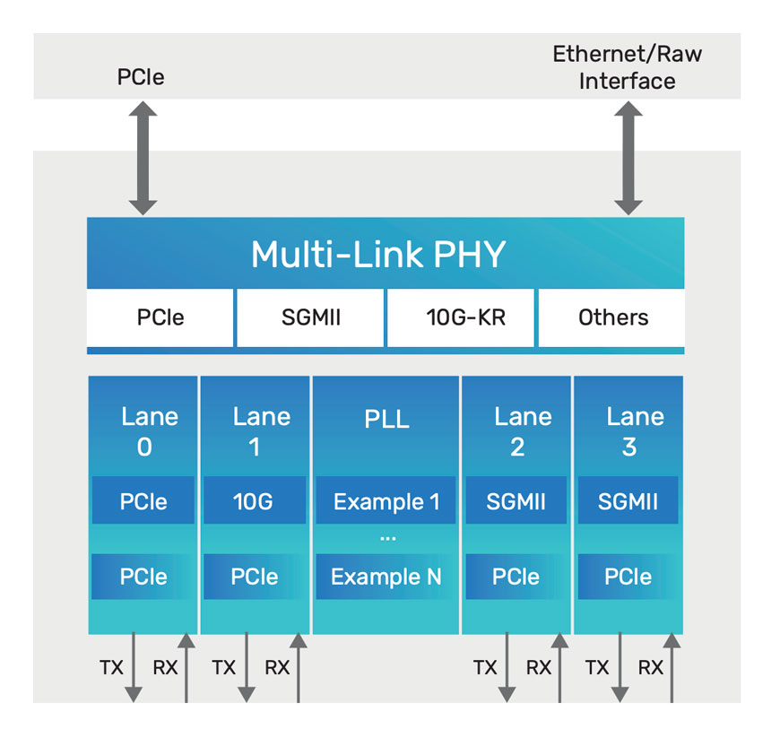
The 16Gbps Multi-Link and Multi-Protocol PHY provides extensive flexibility to mix and match protocols within the same macro. The PHY IP is designed to simultaneously run PCI Express (PCIe), Ethernet, and SGMII/QSGMII on a per-lane basis. Multiple test features are embedded and easily accessible by the end user. A user-friendly graphical interface called EyeSurf provides convenient access to real-time and non-destructive eye scope and bathtubs for monitoring the bit error rate (BER) and the link performance during live traffic.
The PHY IP is engineered to quickly and easily integrate into any SoC, and to connect seamlessly to a Cadence controller for full flexibility. This minimizes the time and risk of device development. It offers SoC integrators the advanced capabilities, flexibilities, and support for advanced, high-performance designs. The Cadence IP is silicon proven for leading-edge process nodes and has been extensively validated with multiple hardware platforms.
Benefits
-
 Silicon proven and fully characterized PHY
 - Seamless integration inside customer's SoC
- Ease-of-use—maximum flexibility and reconfigurability
- Faster to integrate, bring up, and support
Key Features
- High-performance PHY for data center applications
- Low-latency, long-reach, and low-power modes
- Wide range of protocols that support networking, storage, and computing applications
- Multi-Link PHY—mix protocols within the same macro
- EyeSurf—non-destructive on-chip oscilloscope
- Extensive set of isolation, test modes, and loop-backs, including APB and JTAG
- Supports 16-bit, 20-bit, and 32-bit PIPE and non-PIPE interfaces
- Selectable serial pin polarity reversal for both transmit and receive paths
Product Details
The Cadence IP for 16Gbps Multi-Link and Multi-Protocol PHY provides performance, reliability, and robustness for the most demanding applications.
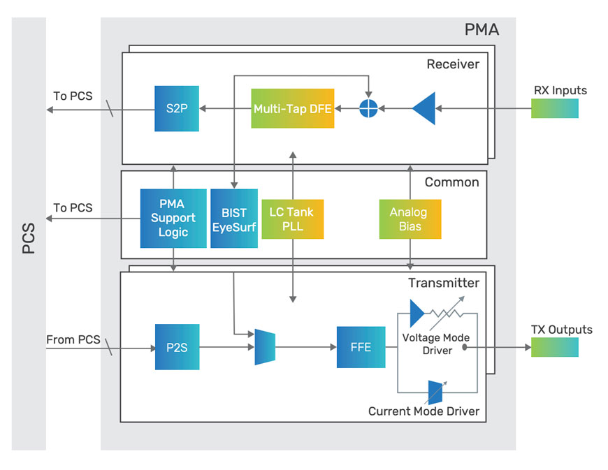
The IP is a hard PHY macro with a physical media attachment (PMA) layer and a soft physical coding sublayer (PCS) available for various processes. The PHY supports long-reach (LR) backplane with insertion loss in excess of 30dB. It is specifically optimized to minimize end-to-end latency and power. Low-power modes are also supported (ex. PCIe L1 substrates, etc.) for energy-efficient applications. For robustness, the PHY operates from -40°C to 125°C, features superior ESD protection, and exceeds the stringent reliability requirements of data center applications.
The PCS complies with the latest PCIe PIPE specification and provides support for the dynamic equalization features of different interface protocols. The IP is designed for handling multiple protocols on one single PHY macro (see table below).
PHY Architecture
The 16Gbps Multi-Link and Multi-Protocol PHY is designed with a multi-link lane-based architecture, providing greater control over floorplanning, placement, packaging, and I/O integration than other hard PHY solutions, while maintaining the reliability and ease of use associated with GDSII macros.
Cadence can deliver various configurations of the IP to meet your design requirements.
Availability
The Cadence IP for 16Gbps Multi-Link and Multi-Protocol PHY is available with various configurations and supports the following protocols:
| Protocol | Data Rate (Gbps/Lane) |
|---|---|
| PCIe 4.0/3.1/2.0/1.0 | Up to 16 |
| 10G-KR | 10.3125 |
| QSGMII/SGMII | 5/1.25 |
Related Products
- Design IP for PCIe 1.0, 2.0, 3.1, and 4.0 Controller
- 10Gbps Multi-Link and Multi-Protocol PHY IP
Deliverables
- Integration Views
- LEF, LIB, DRC/LVS/ANT/ESD reports, Verilog behavioral model, GDSII, CDL, and power models
-
- Soft PHY logic RTL wrapper
- Synthesizable RTL for PCIe PCS
- Synthesis and static timing constraint scripts
-
- DFT
- Verilog netlists with SS/FF, CTL, and BSDL
-
- High Volume Manufacturing (HVM) kit
- Reference Verilog testbenches used for generating SoC-level VCD ATE test patterns for PHY
-
- IBIS-AMI kit
- Documentation
- Hardware and software user guides
- XML
- Integration guide (DFT/ATPG, digital, analog, and package/board)
-
- Testboards available on demand
For more information, visit Design IP.