Brochure
112Gbps ELR SerDes IP for TSMC 5nm
Overview
Overview
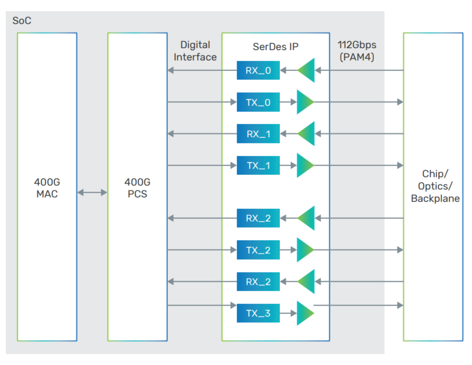
The Cadence 112Gbps Multi-Rate Extended Long-Reach (ELR) PHY IP for TSMC 5nm operates at 56-112Gbps using PAM4 modulation or 1-56Gbps using NRZ. This IP enables high-speed communications between chips, backplane, and long-haul optical interconnects by converting between parallel data and extremely high-speed serial data streams with improved signal reliability. The ELR PHY provides additional performance margin to high-loss and reflective channels by incorporating reflection cancellation and enhanced digital signal processing. The area- and poweroptimized design is ideal for high port-density applications that require ELR performance.
The quad-lane multi-rate PHY IP supports flexible data rate from 1-112G with its ultra-low jitter two-stage PLL architecture. An integrated microcontroller allows for fully autonomous startup, adaptation, and service operation without requiring ASIC intervention. A programming and observation interface is provided via a parallel bus with MDIO-style addressing (port, device, address).
There are several comprehensive on-chip diagnostic tools that enable testability and easy debugging. A post-equalized histogram is available for accurate estimation of bit error rate (BER) even in the absence of actual bit errors. Vertical eye statistics can be logged to allow optional optimization of the device settings. The Channel Estimator hardware allows the accurate measurement of the channel response to assess package, connector, and trace characteristics.
Benefits
-
 Best-in-class DSP supports ELR lossy and reflective channels
 - Small area and low power is ideal for high port-density applications
- Beach-front optimized floorplan allows north-south and east-west SoC edge placement
- Comprehensive on-chip diagnostic features make system testing/debugging quick and easy
Key Features
- TSMC 5nm FinFET CMOS Process
- Power-optimized for ELR and LR links
- Integrated BIST capable of producing and checking PRBS
- 56-112Gbps PAM4 or 1-56Gbps NRZ data rates
- Compact footprint for high-density designs
- Fully autonomous startup and adaptation without requiring ASIC intervention
Product Details
There are four instances of the transmitter and the receiver in the IP.
Transmitter
The transmitter (TX) includes standard encoding, a DAC (microcontroller auto-calibrated) that converts digital signals to an analog output, with a digital FIR filter for waveform pre- emphasis. The transmitter drives a 100Ω differential output with adjustable swing.
Receiver
The receiver (RX) includes an analog front-end, an ADC (microcontroller auto-calibrated) that converts the analog input to digital signals, a DSP equalizer, and standard decoding.
Built-In Self Test (BIST)
The TX may be configured to transmit data from an internal PRBS generator using a list of selectable patterns. The RX may similarly be configured to deliver decoded bits to an internal self- synchronizing PRBS checker to count bit errors in the data stream. Received data may be looped back to the transmitter (see Figure 2).
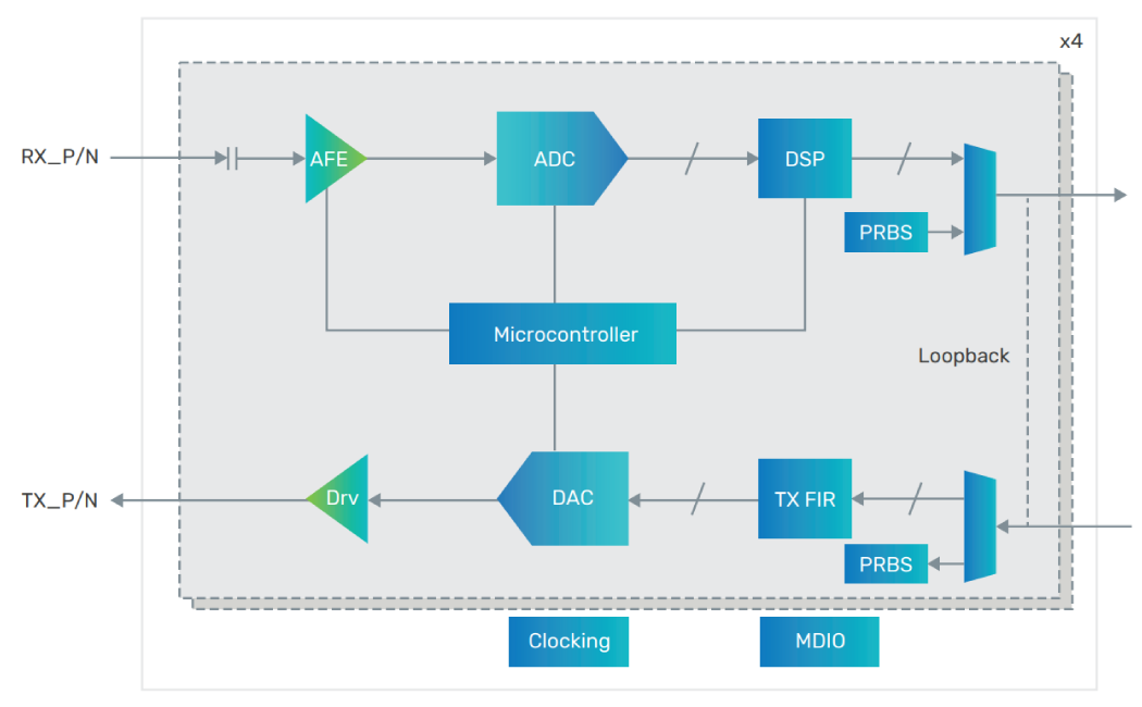
Clocking and Reference Clocks
All timing is derived from an external clock reference via an internal global PLL with separate lane PLLs and phase interpolators for the TX and RX lanes. The RX timing is locked to the incoming data, while the TX timing reference may be configured to derive either from the external reference, or optionally from the RX timing.
Deliverables
- GDS II macros with abstract in LEF
- Verilog post-layout netlist
- STA scripts for use at chip or standalone PHY levels
- Liberty timing model
- Verilog models of I/O pads, and RTL for all PHY modules
- Verilog testbench with memory model, configuration files, and sample tests
- Documentation, including integration and user guide, release notes
- Verification IP setup files
For more information, please visit Design IP.