Brochure
10Gbps Multi-Link and Multi-Protocol PHY IP
Overview
Overview
SerDes requirements for system-on-chip (SoC) designs are becoming increasingly demanding and must support increasing numbers of protocols that must be optimized for cost-and power-sensitive mobile, wireless IoT, consumer, and automotive designs.
The Cadence 10Gbps multi-protocol PHY IP provides a flexible PHY IP that simplifies the design process without compromising performance, power, or silicon die area (PPA). The PHY IP is a lower-active and low-leakage power design crafted for mobile, wireless IoT, consumer, and automotive designs.
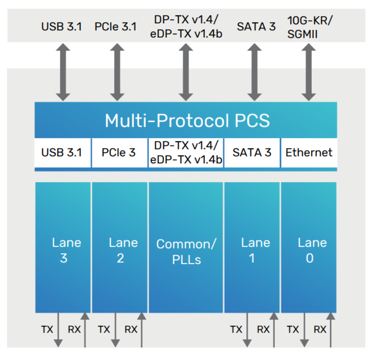
The PHY IP is designed for multi-protocols running on single PHY macro and is compliant with USB 3.1, PCI Express (PCIe) 3.1, DisplayPort TX v1.4, Embedded DisplayPort TX v1.4b, SATA 3, QSGMII, and SGMII specifications. The PCS complies with the PIPE 4.2 interfaces, and provides support for the dynamic equalization features of different protocols.
The PHY IP is architected to quickly and easily integrate into any SoC, and to connect seamlessly to Cadence or third-party PIPE-compliant controllers. It provides a cost-effective, versatile, and low-power solution for demanding applications. It offers SoC integrators the advanced capabilities, flexibility, and support that meet the requirements of high-performance designs.
The PHY IP is part of the comprehensive Cadence Design IP portfolio comprised of interface, memory, analog, and system and peripheral IP.
Benefits
Key Features
Product Details
The PHY IP is a hard PHY macro available for TSMC processes. I/O pads and ESD structures are included. It is designed to easily integrate with a Cadence Controller IP for PCIe and USB, or any third-party controller with a PIPE-compliant interface. Raw SerDes interface is adopted for Ethernet and DisplayPort protocols.
PHY Architecture
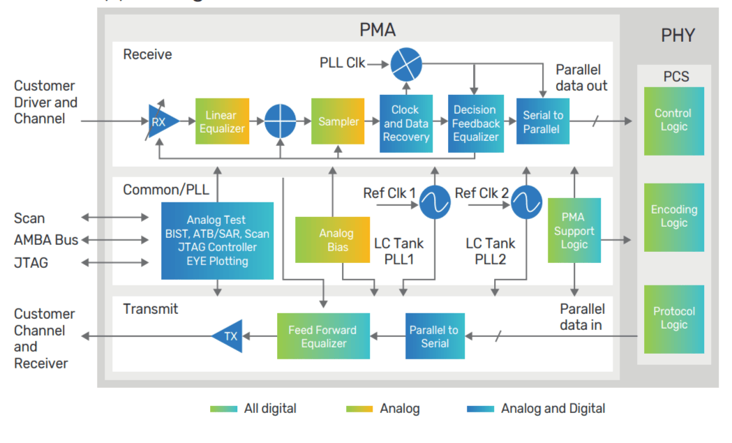
The PHY IP macro consists of a Physical Media Attachment (PMA) layer and a Physical Coding Sublayer (PCS). The Multi-Protocol and Multi-Link architecture PHY IP is highly configurable, allowing the PHY to be easily configured to your specific needs.
The PHY IP is designed with a lane-based architecture featuring one common support for up to eight lanes, providing greater control over floorplanning, placement, packaging, and I/O integration than other hard PHY solutions, while maintaining the reliability and ease of use associated with GDSII macros.
The PCS portion of the PHY provides the control, encoding, and protocol logic. The architecture partitions the PMA core into different primary sub-modules: common PLL, transmitter, and receiver lane modules. The PMA block provides the transmit, common PLL, and receive functions. The common PLL module also provides the interface between SCAN, Arm AMBA Bus, and JTAG and Analog Test including BIST, ABT, Scan, JTAG control, eye plotting, and PMA support logic functions.
Availability
The PHY IP is available with support for the following process nodes:
| Process Node | Speed |
|---|---|
| 16FFC | 10.3125Gbps |
| 12FFC | 10.3125Gbps |
| N7 | 10.3125Gbps |
| N5 | 10.3125Gbps |
Deliverables
For more information, visit designip.


