Application Note
Design of a Reduced Footprint Microwave Wilkinson Power Divider with EM Verification
Overview
Overview
This application note describes how to design a microwave Wilkinson power divider with a reduced footprint using the Cadence AWR Design Environment platform, specifically AWR Microwave Office circuit design software and AWR AXIEM 3D planar electromagnetic (EM) analysis software. The entire design presented below covers schematic entry to physical PCB implementation, as well as final EM verification.
The design flow steps include:
-
 Step 1: Circuit Design Using Ideal Transmission Lines
 - Step 2: Impact of a Microstrip Implementation
- Step 3: Equivalent Physical Layout of the Design
- Adding bends
- Accounting for coupling
- AWR Automated Circuit Extraction (ACE) technology
-
- Step 4: Circuit Compaction
Step 1: Circuit Design Using Ideal Transmission Lines
The Wilkinson power divider is a specific class of power divider circuit that can achieve isolation between the output ports while maintaining a matched condition on all ports. A further advantage is that when used at microwave frequencies it can often be made very inexpensively because the transmission line elements can be printed on the PCB. It uses quarter wave transformers, which can be easily fabricated as quarter wave lines on the PCBs. In this example, the Wilkinson power divider is first implemented using ideal transmission lines, as shown in Figure 1.
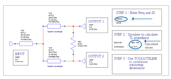
In the first stage, the designer can use ideal transmission line models based on the required electrical length at the center frequency (2GHz) for the given design and its characteristic impedance (50ohms). In this example, the schematic includes the simple equations used to calculate the impedances for the transmission line and the resistor. Pressing the F6 function key will update the results of these equations without running a simulation and the calculated values will appear. The physical attributes can be obtained once a substrate material is identified. The substrate used in this design has the following electrical/ physical properties:
Dielectric constant Er = 3.66
Tangential loss = 0.0035
Thickness H = 0.762mm
Conductor thickness (1/2 oz. copper) = 0.01778
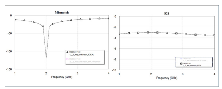
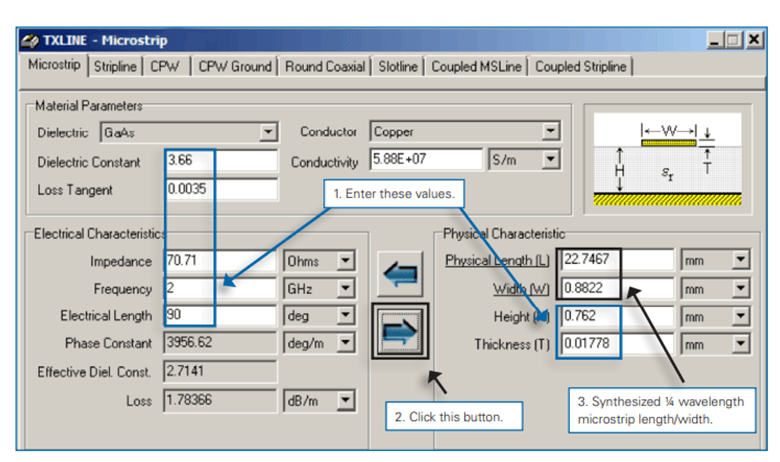
Simulate and display the results (Figure 2) of the power divider modeled using ideal transmission lines. To continue to improve the design, synthesize the lengths and widths of the microstrip lines with the calculated values. This is done using the TX-LINE freeware program that’s embedded within AWR Microwave Office software.
In TX-LINE, enter the substrate properties, the impedance of the transmission line that was calculated (70.71ohms), and the electrical length of the quarter wavelength (90 degrees), as shown in Figure 3. The 50ohm line width is synthesized in the same way.
Step 2: Impact of a Microstrip Implementation
After the microstrip line length/width has been synthesized, an updated schematic is created. Key features of AWR Microwave Office software used in the schematic are iCells and Xmodels (MTEEX$). The “$” postfix in the MTEE model is an intelligent cell. There is no need to explicitly specify the widths of the microstrip lines connected to it: it automatically detects the widths of the lines and builds the correct model of the T junction. The “X” postfix in the MTEE model signifies that the model is an EM-based model.
Also used in the schematic is the MTRACE2 element. This is a microstrip with two additional parameters, DB and RB. If these are set to zero, then it is a straight, single microstrip element. Otherwise, the MTRACE2 may contain a series of MLINS and MBENDS, as defined by how it is routed.
The MTRACE2 is deployed for the two one-quarter wavelength microstrips so that the lines can be bent in the layout environment. The bends and microstrip sections are added automatically to the MTRACE2 model, simplifying the design process by avoiding the need to explicitly describe each microstrip section in the schematic.
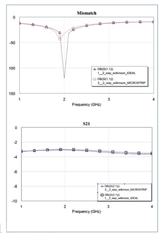
Since the two one-quarter wavelengths track each other in width and length, one of the MTRACES can be set to have the following W and L parameters: W=W@MTRACE2.X1, L=L@MTRACE2.X1. A comparison of the insertion loss versus frequency from Ports 1 to 2 between the power divider based on an ideal electrical transmission line and an ideal physical line is shown in Figure 4. This plot shows a loss of approximately 3dB, which would be expected for a two-way splitter.
Step 3: Equivalent Physical Design of the Layout
The next step is to perform the physical board layout of the design, minimizing the board area without compromising performance and considering the effects of coupling and other parasitics. This is done by using the PLACE ALL command located in the Edit menu at the top of the AWR Microwave Office window. Remember that there are two MTRACES in this schematic, MTRACE2.X1 and MTRACE2.X2. Make MTRACE2.X2 track MTRACE2.X1 by setting the parameters of MTRACE2.X2 as follows:
W=W@MTRACE2.X1
L=L@MTRACE2.X1
DB=DB@MTRACE2.X1
RB=RB@MTRACE2.X1
The next phase of development is to route the quarter-wave length branches of the power divider. AWR Microwave Office software offers a few useful features, including SNAP TO FIT routing of MTRACE2 while maintaining physical length, and STRETCH TO FIT. Red “rubber band” lines indicate electrical connections, the points in the layout elements that need to be connected physically, and once they are connected, the red lines will disappear. Multiple lines can be connected by selecting them and clicking the SNAP TO FIT button.
Adding bends
Once the microstrip elements are connected physically, the red lines disappear. Now the MTRACES can be bent and the entire power divider layout completed.
In the next phase, bends are added to the MTRACES. Note that in the schematic symbol of MTRACE2, there is a “/” symbol at one of the ports. This represents Port 1 of the element. Electrically, it does not matter if the MTRACE is connected with Port 1 on the other side. However, Port 1 is where the routing of the MTRACE in the layout environment is begun. In the layout editor, Port 1 is indicated by a blue triangle on one of the ends of the MTRACE layout.
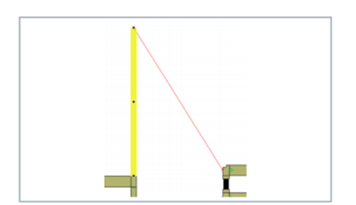
The first step in adding bends to the line is to double click on the MTRACE. Three black dots (handles) appear on the MTRACE, as shown in Figure 5. Move the mouse cursor to Port 1 (blue triangle) of the MTRACE. The mouse cursor will become a doublearrow sign when it is at Port 1.
Since the length of the MTRACE is calculated, it is necessary to maintain the line length when the bends are added. In this situation, hold down the SHIFT key throughout the routing process. While the SHIFT key is held down, double-click on Port 1. Begin routing the line and bending it. Be sure the SHIFT key is held down, otherwise the line length will be changed after the routing process is completed.
Click when finished routing the MTRACE. Note that in this case, three bends have been added to the top MTRACE. The bottom MTRACE has the same number of bends (and same angles) because the DB and RB have been set to track the top MTRACE (in other words, MTRACE2.X1).
To flip the bottom MTRACE to the correct direction, select it, right click, and select FLIP. In the schematic, note that the length of the MTRACE has been maintained. Double click on the MTRACE element and notice that the DB and RB parameters now indicate the number of bends added and the associated angles.
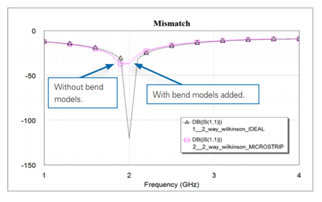
Simulate the circuit again. It can now be seen in Figure 6 that there is a slight change of S-parameters due to the added bend models in the MTRACE. Align the input 50-ohm line, the MTEE$ junction, and the two MTRACES and snap them together. Then connect the MTRACES to the resistor
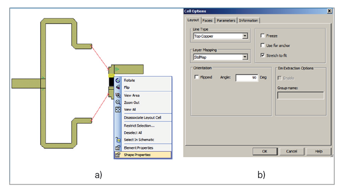
The entire layout is a loop. In order to connect the MTRACES exactly with the resistor’s solder pads, make one of the solder pads stretchable. This is done by right clicking on the solder pad (Figure 7), selecting SHAPE PROPERTIES, and then enabling STRETCH TO FIT. Select all (CTRL-A) and snap all of the elements together. One of the solder pads stretches itself so that the connection is made. This will introduce a very high inductive parasitic that is not desired. To fix this, go to OPTIONS/LAYOUT OPTIONS and set to AUTO SNAP mode.
The top MTRACE can now be adjusted to minimize the length of the solder pad. Double click on the MTRACE and move the handles (black dots) as appropriate. The layout of the power divider is now complete. Re-simulate the circuit and see the effects of the bends and the slightly modified solder pad length.
Accounting for coupling
The next step is to determine how to handle couplings between sections in MTRACE. MTRACES are basically a series of MBENDs and MLINs. The mutual coupling between MLIN sections are not included in the simulation. To account for the mutual coupling, there are two options, the first of which is EM simulation. EM simulators should be used as a verification tool, so in this case, where moving the lines around and quickly analyzing the coupling effects is desired, EM simulation is not the best choice. A design tool is needed that can quickly extract the coupling effects and simulate within seconds.
Automated circuit extraction
The second option is to use AWR’s ACE automated circuit extraction technology. The AWR ACE design tool very quickly extracts highly accurate high-frequency models of the layout, including coupling effects. The tool can be used to make changes to the layout and evaluate the resulting S-parameters while considering coupling issues without having to do a full EM simulation. In this way, RF circuits can be compacted very quickly. EM simulation is only invoked at the end of the design process in order to verify the design.
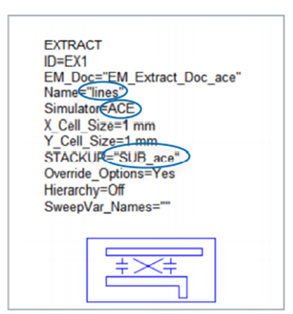
In this example, AWR ACE technology is employed to evaluate the coupling between the microstrip sections. Set the AWR ACE tool by first setting up the STACKUP, then selecting which lines are needed to extract the coupling and, finally, inserting the EXTRACT block. To evaluate the coupling between the microstrip lines, select the two MTRACES and 50ohm output lines and name them “Lines.” The EXTRACT block is then added, referencing the name Lines, and the AWR ACE tool is invoked (Figure 8).
Note that once AWR ACE technology is set up, it is very easy to simulate coupling between microstrip lines. The lines in Figure 9 (red) are being extracted to perform an AWR ACE simulation, so the coupling effects can be considered. In this way, the designer can adjust the layout to the desired size and then an EM simulation can be done on the layout as a final verification.
Step 4: Circuit Compaction
Now the physical design of the power divider is complete, the next objective is to further miniaturize the layout. The power divider that was laid out has the dimensions (DRAW/DIMENSION LINES) shown in Figure 10 and now needs to be evaluated to see if it can be made smaller. By re-routing the MTRACE, an exercise now left to the reader, a smaller layout (Figure 11) can be achieved. Once again, the AWR ACE tool can be deployed to extract the coupling effects that will be taken into account during the layout adjustments and circuit simulation. Line lengths of the MTRACEs can be tuned along with the AWR ACE tool, and, eventually, the AWR AXIEM 3D planar EM simulator is used for final EM verification (Figure 12).

Conclusion
This application note has described the steps for designing a Wilkinson power divider, including design using ideal transmission lines, microstrip implementation, physical design, and circuit compaction. The entire design was done using the Cadence AWR Design Environment platform, specifically AWR Microwave Office software for the design from schematic entry to physical PCB implementation, the AWR ACE tool for evaluating the coupling between the microstrip sections, and AWR AXIEM software for final EM verification.