Application Note
Design of a 10GHz LNA for Amateur Radio Operation Using AWR Software
Couple the mysterious nature of amateur (ham) radio in microwave bands to the lack of store-bought gear that operates in this band and you have the right recipe for a home brew of equipment. So when the design of a 10GHz ham radio station was originally discussed within the amateur radio community, one of the key missing blocks was a good low-noise amplifier (LNA). This application note describes how an LNA was therefore custom made (home brewed) utilizing Cadence AWR Design Environment circuit design software.
Overview
LNA Specifications
The LNA was designed to operate from +12V with at least 18dB of gain, less than 2dB noise figure, and unconditional stability. Linear analysis, design tradeoffs, and tuning were performed with Cadence AWR Microwave Office circuit design software, which contributed significantly to the success of this project. The design steps are detailed in the following section. Since the final radio was to be built entirely at home without the benefit of commercial grade fabrication and assembly tools, some important choices needed to be made at the outset. Among these were:
Design Approach
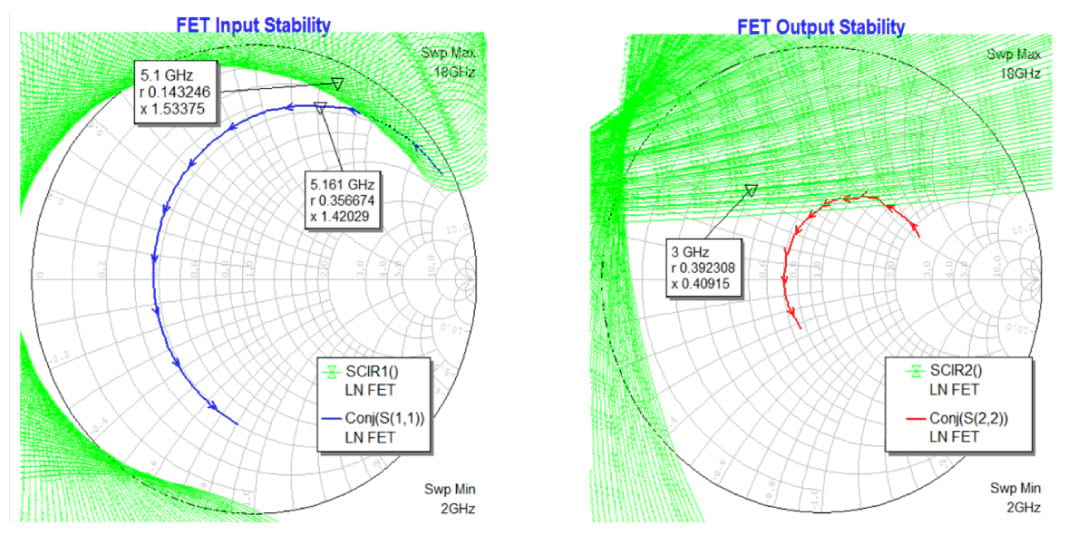
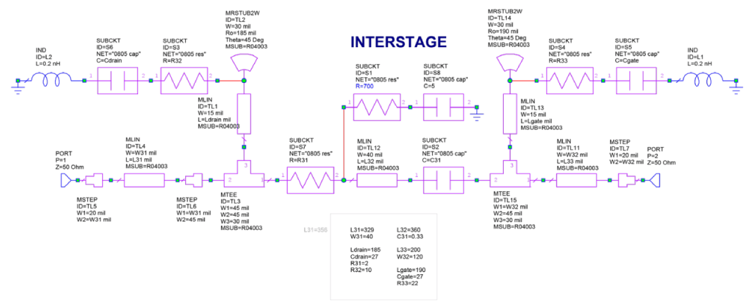
The LNA design utilized FETs operating with 15 to 20mA drain current. In order to gain insight into the stability tradeoffs in the LNA, it was worthwhile looking at inherent stability behavior of these FETs. As can be seen in Figure 1, the plots suggest that series loss at the input and shunt loss at the output will enhance stability. Initially, a single-stage amplifier was designed as a building block in a two-stage amplifier. The actual interstage RF circuit was a cascade of an output network from Stage 1 and the input network from Stage 2 with a phase rotation line inserted between them. This was used to tune the overall two-stage stability performance.
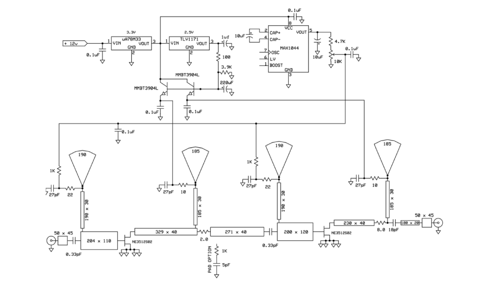
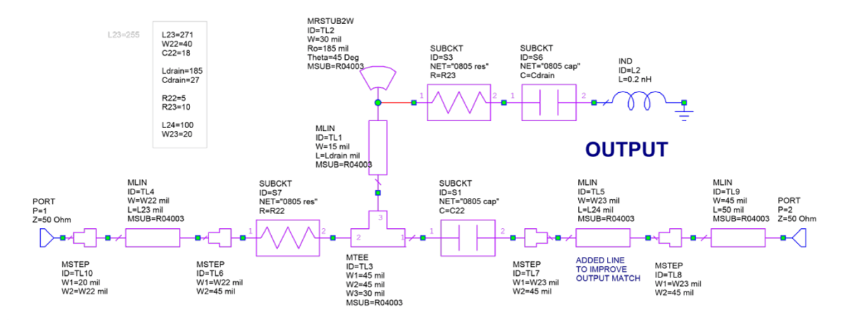
The overall amplifier schematic is shown in Figure 2. Gate and drain bias networks comprise a high impedance ¼λ line that was terminated by a low impedance, bypassed, DC feed circuit. A low impedance (near short circuit) for in-band frequencies was provided by an open-circuit ¼λ radial stub. The DC feed path is also decoupled and damped by series resistance.
The +12V DC input was first dropped to a regulated 3.3V rail, followed by a 2.5V regulator. The 3.3V rail fed the collector of two emitter follower pass transistors for drain supply of the two LNA FETs. The 3.3V rail also powered the negative voltage generator integrated circuit (IC) (MAX1044) for the LNA FET gate bias. The 2.5V regulator provided a base reference voltage for the emitter followers. At turn on, the rise in base voltage was delayed by an RC circuit to sequence the gate negative supply before the drain positive supply. The emitter followers also provided supply path isolation between RF stages.
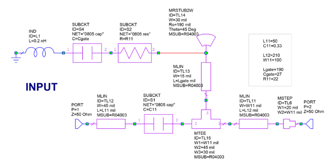
The RF cascade is represented in Figure 3. Details of the input, interstage, and output RF matching networks can be seen in Figures 4, 5, and 6.
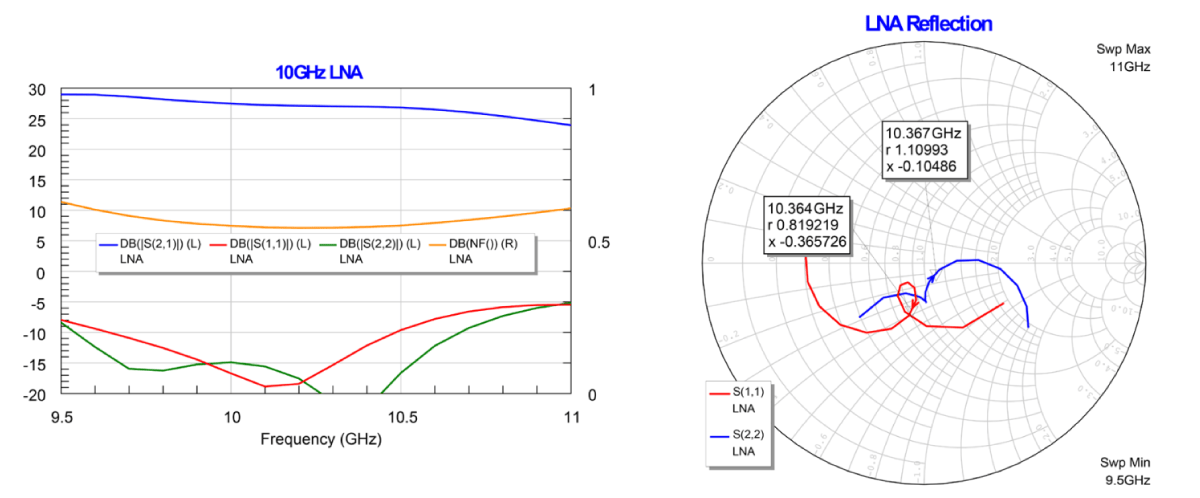
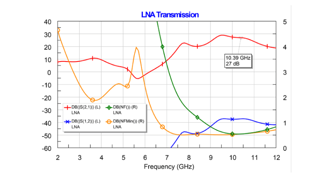
The overall simulated gain, port match, and noise performance are shown in Figures 7 and 8. For ham radio operation, the frequency region of most interest was 10.368GHz. The overall swept performance was not extremely narrow. Figure 8 shows a wide (2.5 octave) sweep. No extreme peaks in gain are seen at lower, out-of-band frequencies.
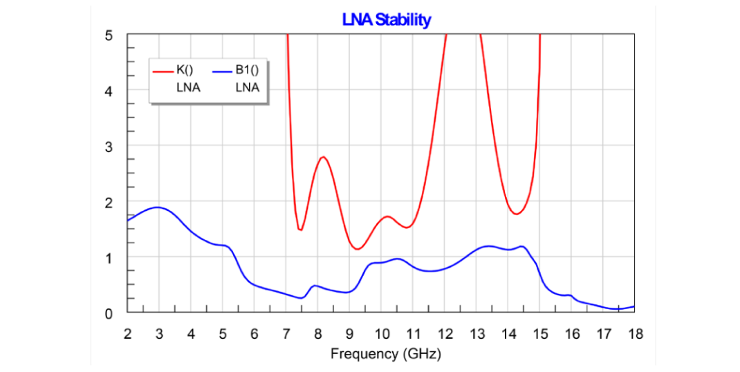
The well-behaved out-of-band behavior displayed in Figure 8 suggests that the stability of the LNA will be good. A detailed stability analysis confirmed this. For unconditional stability, Rollett’s K factor had to be greater than unity and the B1 parameter had to remain positive. This can be seen in Figure 9.
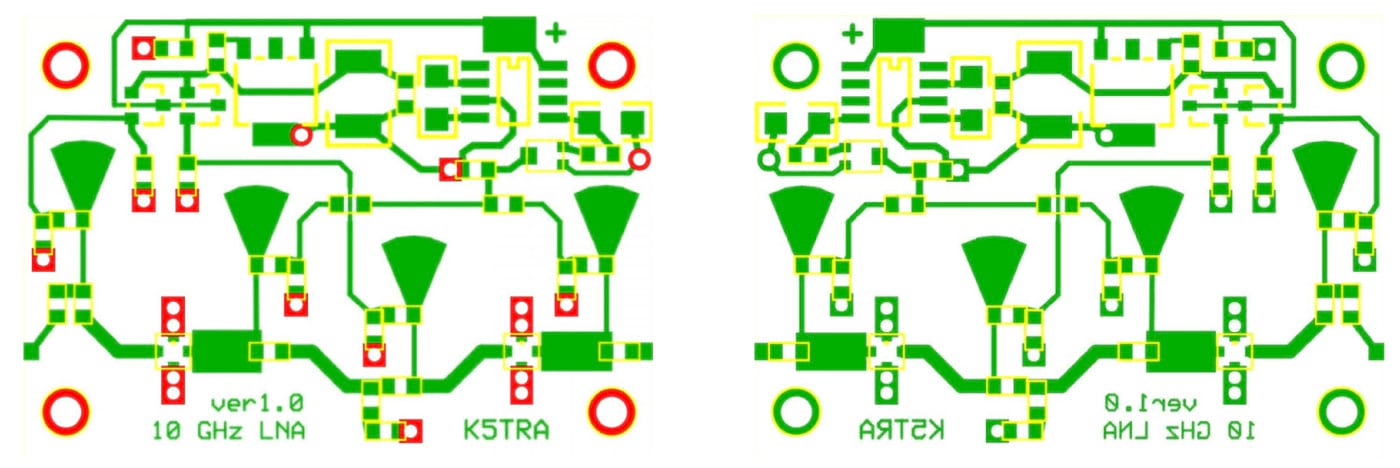
The layout of the designed LNA is shown in Figure 10. The RF input is on the right and output is on the left edge. Layouts were done for both NE3512S02 and NE3503M04 pHEMTs. Figure 10 also shows the NE3512S02 pattern (and its mirror resist for etching).
Construction Process
Construction of the LNA began with resist patterning and etching of the circuit board. The board was then etched in a homemade bubble etcher and finished with a thin tin plate. Via holes were defined with a 35 mil drill. Figure 11 shows the undrilled, etched board placed in the undrilled housing.
With the home-brew board process, it was necessary to solder wires in the through holes at each via location. An interior view of the completed LNA is shown in Figure 11. The input is on the right and output on the left. The 3.3V regulator can be seen on the left wall. The DC circuitry can clearly be seen along the top of the board and the RF amplifier stages on the lower portion. Four small rectangles of Eccosorb can also be seen attached to DC bias feed lines. This was done for practical reasons as insurance against parasitic feedback paths, although likely not needed. As stated earlier, moding suppression was needed in this housing because 10GHz will propagate through a cavity this large. Eccosorb patches were placed on the right and lower side walls as well as on the inside of the cover. Stability behavior was excellent.
The completed LNA can be seen in Figure 11. The measured gain is just over +18dB and the associated noise figure (NF) is near 2dB. While this met the performance targets for use in the 10GHz station, the predicted levels were a bit better. The differences can be attributed to poor line-width control and excess via inductance in the home-fabricated circuit board.
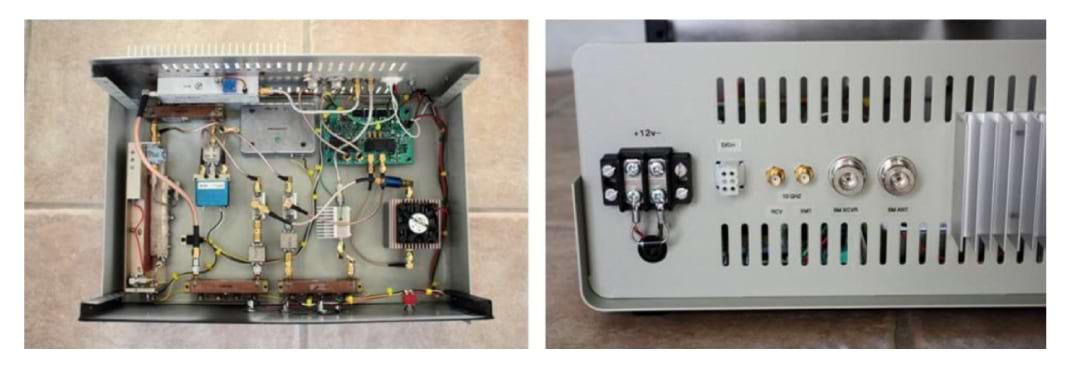
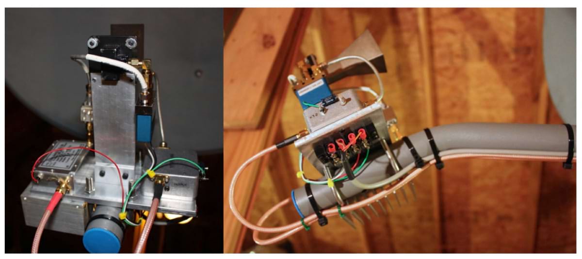
For maximum receiver sensitivity (minimum system noise figure), losses between the dish feed horn and the LNA had to be minimal. Similarly, on the transmit side, losses between the power amplifier and the dish feed horn had to be kept to a minimum. While most of the transmit and receive circuitry was located in the transverter (also home brew) shown in Figure 12, the LNA and PA were mounted with the feed horn at the dish. Figure 13 shows two views of the LNA, coaxial relay, PA, isolator, and feed horn.
Conclusion
Because store-bought ham radios are not available for microwave bands, this application note has described the custom design of a 10GHz LNA that enables the use of amateur radio within such a band. A key block of the final home-brew ham radio, the LNA was realized using AWR Microwave Office software. This enabled the designer to tune the design while simultaneously watching gain, match, NF, and stability.
On-air results for the final product have been outstanding. There are half a dozen ham radio operators with 10GHz stations within 50 miles of this designer (author of application note) and they can all communicate on a routine basis. With a hilltop location and good view in all directions, the most distant of these local hams is located 45 miles away. The most exciting contact occurred early one morning when ducting and scatter conditions supported unusually long path propagation. The designer was able to contact a station in Allen, Texas (north of Dallas), 213 miles away.
For more information on this topic: 10 GHz Transverter, Dish-Feed, & Instrumentation.
Acknowledgement
Special thanks to ham radio operator Tom Apel (K5TRA) for his contributions to this application note.

