Application Note
AWR Software for the Design of MIMO and Phased Array Antenna Systems
Phased array antennas are becoming popular for a variety of applications such as automotive driver assist systems, satellite communications, advanced radar, and more. The complexity and cost issues involved in developing communications systems based on phased array antennas are being addressed through new functionalities in electronic design automation (EDA) software that support designers with the means to develop new system architectures and component specifications, as well as implement the physical design of individual components and verify performance prior to prototyping.
Overview
Design Overview
This application note discusses these trends and presents recent advances in EDA tools for phased array-based systems. While actively-steered phased array antennas have many advantages, they are extremely complex and their production, especially non-recurring development costs, is significantly higher than for conventional antenna design. As the industry shifts toward highly integrated phased array systems, it is critical for in-house systems experts to work closely with hardware developers, with both fully exploring the capabilities and tradeoffs among possible architectures and integration technologies. In addition, a start-to-finish design flow made possible with EDA software has become critical in moving beyond the initial system simulation, which is focused on early architecture definition, to the development of link budgets and component specifications.
A preferred phased array system design flow manages the start-to-finish front-end development, embedding RF/ microwave circuit simulation and/or measured data of radio/signal-processing (behavioral) models within a phased array system hierarchy. Such software enables the system designer to select the optimum solution, ranging from hybrid modules through fully integrated silicon core RF integrated circuit (IC) devices, addressing the specific requirements of the targeted application. Perhaps more importantly, a system-aware approach, carried throughout the entire phased array development cycle, enables the team to continually incorporate more detail into their predictive models, observe the interactions between array components, and make system adjustments as the overall performance inadvertently drifts from early idealized simulations.
Design failure and the resulting high costs of development are often due in part to the inability of high-level system tools to accurately model the interactions between the large number of interconnected channels, which are typically specified and characterized individually. Since overall phased array performance is neither driven purely by the antenna nor by the microwave electronics in the feed network, simulation must capture their combined interaction in order to accurately predict true system behavior. Circuit, system, and electromagnetic (EM) co-simulation enables verification throughout the design process.
Phased Array Design Flow
A leading phased array design flow is available with Cadence AWR Visual System Simulator (VSS), the system-level simulator that operates within the Cadence AWR Design Environment platform. The simulator provides full system performance as a function of steered-beam direction, inclusive of the antenna design and the active and passive circuit elements used to implement the electronic beam steering. System components can be modeled in greater detail using Cadence AWR Microwave Office circuit simulation, inclusive of EM analysis for antenna design and passive device modeling using Cadence AWR AXIEM 3D planar and Analyst 3D finite-element method EM simulators.
These tools are fully integrated into the AWR Design Environment, supporting seamless data sharing within the phased array hierarchy. Furthermore, individual antenna designs can be generated from performance specifications using the Cadence AWR AntSyn antenna synthesis and optimization module, with resulting geometries imported into Cadence AWR AXIEM or Analyst software for further EM analysis and optimization.
Highlights of phased array analysis in AWR VSS software include:
-
 Automate/manage the implementation of beamforming algorithms and determine phased array antenna configuration from a single input/output block
 - Accomplish array performance over a range of user-specified parameters such as power level and/or frequency.
- Perform various link-budget analyses of the RF feed network, including measurements such as cascaded gain, noise figure (NF), output power (P1dB), gain-to-noise temperature (G/T), and more
- Evaluate sensitivity to imperfections and hardware impairments via yield analysis
- Perform end-to-end system simulations using a complete model of the phased array
- Simulate changing array impedance as a function of beam angle to study the impact of impedance mismatch and gain compression on front-end amplifier performance
Defining Phased Array Configurations
Specifications for any phased array radar are driven by the platform requirements and the intended application. For example, weather observation, which has relied on radar since the earliest days of this technology, most commonly uses airborne surveillance radar to detect and provide timely warnings of severe storms with hazardous winds and damaging hail. The weather surveillance radars are allocated to the S (~ 10cm wavelength), C (~ 5cm wavelength), and X (~ 3cm wavelength) frequency bands. While the shorter wavelength radars provide the benefit of a smaller antenna size, their radiated signals are significantly affected by atmospheric attenuation.
Requirements for 10cm wavelength (S-band) weather surveillance radars, based on years of experience with the national network of non-Doppler radars (WSR-57), are shown in Table 11.
| 1.1. Surveillance | ||
| 1.1.1 Range | 460 km | |
| 1.1.2 Time | < 5 minutes | |
| 1.1.3 Volumetric coverage | hemispherical | |
| 1.2. SNR | > 10 dB, for Z. 15 dBZ at r = 230 km | |
These requirements showcase some of the application-specific metrics that drive range, frequency, antenna size, and gain. They represent the starting point for the system designer, who also will weigh cost and delivery concerns and available semiconductor and integration technologies when considering possible architectures and defining individual component performance targets.
The AWR VSS software provides system designers with the capabilities needed to convert these requirements into hardware specifications and work out the initial design details. Starting with the phased array configuration, the AWR VSS software is able to represent thousands of antenna elements with a single model, enabling the antenna design team to quickly produce radiation patterns with basic array properties such as number of elements, element spacing, individual element gain or radiation pattern (imported measured or simulated antenna data), array configuration, and gain taper. The model, shown in Figure 1, allows designers to specify the array’s physical configuration based on various standard lattice and circular geometries, as well as custom geometries.
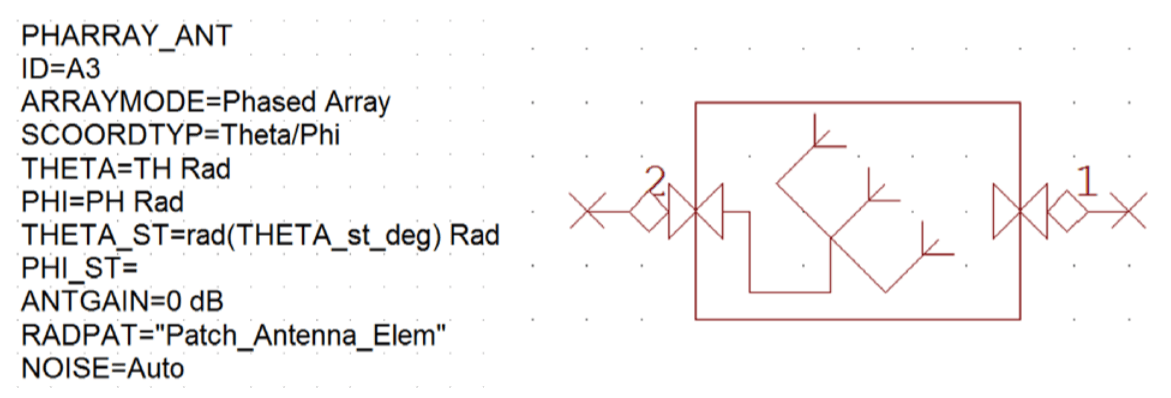
The array behavior is easily defined through a parameter dialog box or a data file containing configuration parameters such as gain and phase offset, theta/phi angles of incidence, number of elements in both X/Y locations (length units or lambdabased), spacing, and signal frequency. This model greatly simplifies early exploration of large-scale phased array configurations and individual antenna performance requirements versus the old method of implementing such a model using basic individual blocks, where array sizes were generally limited to several hundred elements, each modeled as a single input/single output block.
Figure 2 shows a portion of the AWR VSS parameter dialog box used to quickly define an antenna-array architecture using standard or custom geometries. The lattice option allows configuration of the phased array in a lattice pattern using the number of elements along the X and Y axes, NX and NY, element spacing along these axes, dx and dy, and gamma, the angle between these axes. Setting gamma to 90° results in a rectangular lattice, while setting it to 60° creates a triangular lattice.
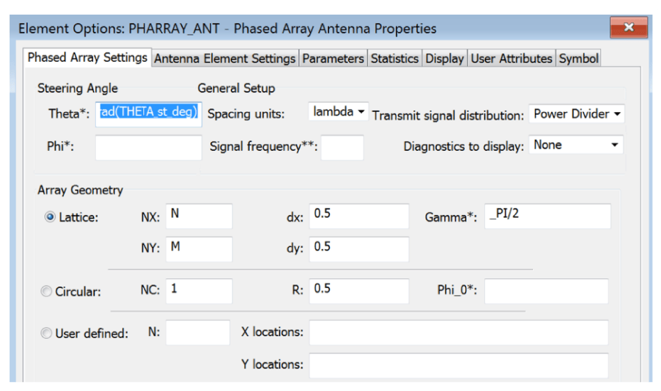
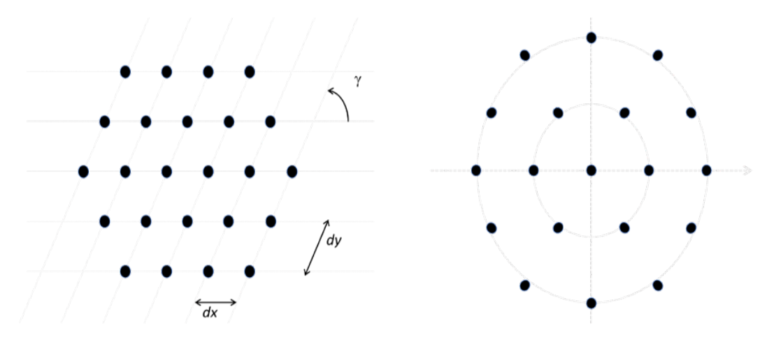
Any positive value for gamma may be used to configure the lattice, while the circular option enables configuration of circular phased arrays with one or more concentric circles. The number of elements in each concentric circle and the radius of each circle can be defined as vectors by variables NC and R. Examples of lattice and circular array configurations are shown in Figure 3.
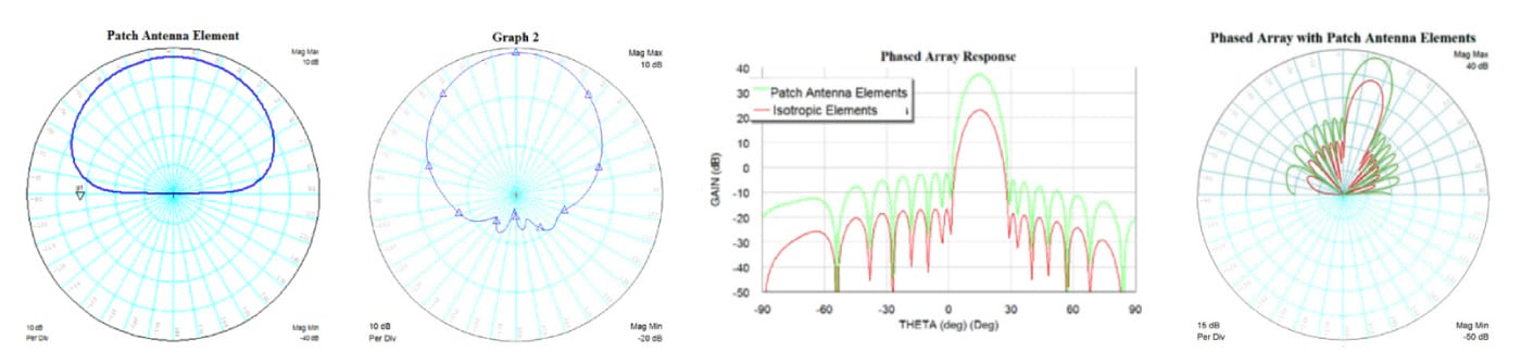
To demonstrate some of the capabilities of the phased array model, an example project was constructed showing two 15x5 element arrays operating at 2.99GHz (Figure 4).
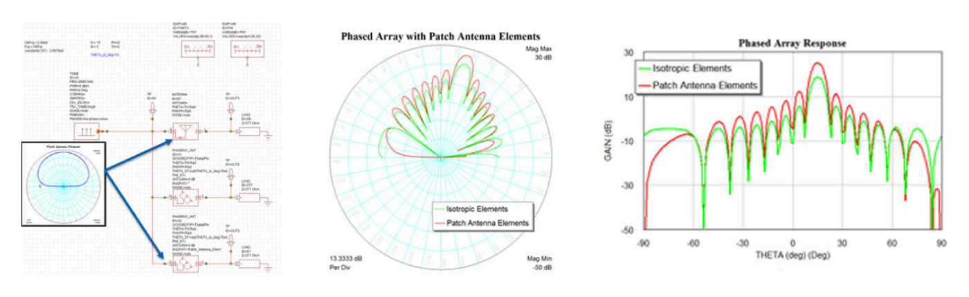
One model represents an array of lossless isotropic antennas defined simply by setting the antenna gain to 0dBi, while the elements of the other array utilize a data set containing the radiation pattern of a single simulated patch antenna. Both arrays use a lattice configuration with a 1/2-wavelength spacing between elements and uniform gain tapering, explained in more detail below. For the simulation shown, the steering angle (theta) was set to 15°. Note that the antenna and phased array blocks support specifying the signal direction using U/V coordinates as well as theta/phi angles (Figure 5).
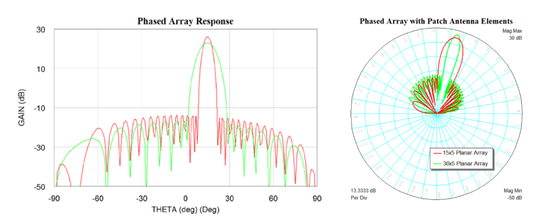
The AWR VSS array model provides antenna designers with a rapid and straightforward tool to observe key antenna metrics, providing a means to examine the main beam and side lobe behavior as a function of any number of variables, including array size and configuration, gain versus steering angle, and the occurrence of grading lobes as a function of element spacing and/ or frequency. From these results the array design team can develop an optimum configuration for the given requirements such as range and overall array physical size. In addition, the team can provide design targets for the individual antennas and incorporate subsequent antenna simulation results back into the array analysis.
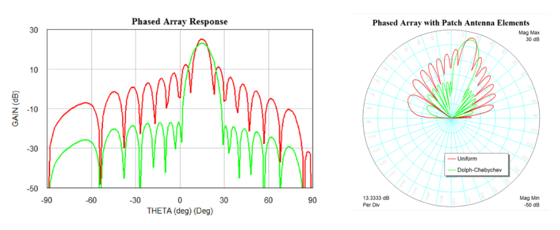
Changing the amplitude excitation through gain tapering is often used to control beam shape and reduce the side-lobe levels. A number of commonly used gain tapers are implemented in the phased array block. Gain taper coefficient handling defines whether the gain taper is normalized or not. If it is, the taper is normalized to unit gain. Standard gain tapers implemented in the phased array model include Dolph-Chebyshev, Taylor Hansen, and uniform. The earlier example (5 x 15 element patch array) was re-simulated with uniform versus Dolph-Chebyshev gain tapering to understand the impact on the main beam and side lobes, as shown in Figure 6. In addition, the user can define custom gain tapers by specifying the gains (dB) and phases for each array element.
Individual Antenna Design
In the previous example, the 5 x 15 array presented the radiation patterns for an ideal isotropic antenna (gain = 0dBi) and a simple patch antenna. In addition to the array configuration itself, the design team would likely want to specify the radiation pattern and size constraints for the individual antenna elements. This operation can be performed using the synthesis capabilities in AntSyn software, which uses an EM solver driven by proprietary evolutionary algorithms to explore multiple design options based on antenna specifications defined by the engineer. These specifications include typical antenna metrics, physical size constraints, and optional candidate antenna types.
In Figure 7, AntSyn software creates antenna geometries from its database of design types and then applies EM simulation and its unique evolutionary optimization to modify those designs and achieve the required electrical performance and size constraints. A run-time update of the design types under investigation is listed, along with a star rating system to indicate which designs are close to achieving the desired performance. Promising designs can then be exported to AWR Design Environment.
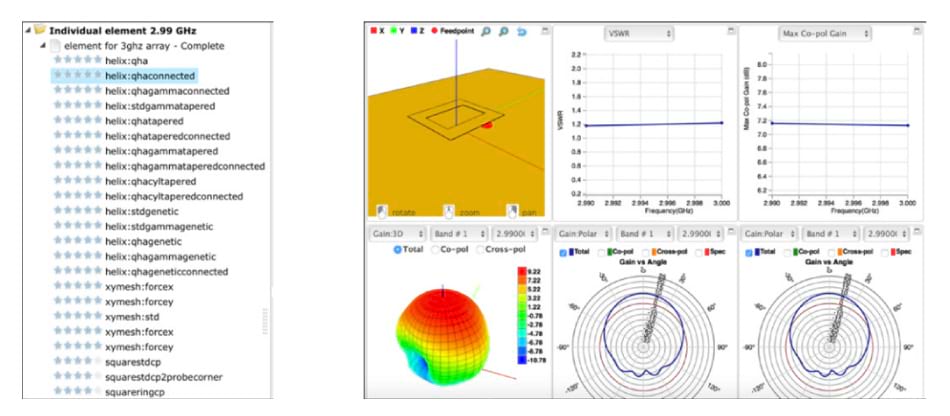
Due to its relatively small size and easy fabrication, a square-ring patch antenna was chosen from the potential antennas created by AntSyn software. The antenna was exported using the AWR AXIEM options and then imported into a new AWR AXIEM EM structure in the initial phased array project. The re-simulated antenna is shown in Figure 8.
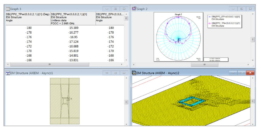
This simulation provided the antenna pattern to replace the original patch antenna used in the 5 x 15 phased array with the new antenna pattern shown in Figure 9. The new phased array results for both the original antenna (red trace) and the square-ring patch (green trace) are shown in Figure 9 as well.
Modeling Complex Interactions
The mutual coupling between antenna elements affects antenna parameters like terminal impedances and reflection coefficients, and hence, the antenna-array performance in terms of radiation characteristics, output signal-to-interference noise ratio (SINR), and radar cross section (RCS). AWR VSS software includes new capabilities for more accurate simulation of these parameters, including enhanced modeling of element patterns and mutual coupling. The next section of this application note will examine these recent advances in advanced phased array modeling, including accurate representation of the feed structure.
As mentioned, in AWR VSS software, designers can define gains or full radiation patterns for each antenna element in the phased array. This enables them to use different radiation patterns for internal, edge, and corner elements of the phased array (Figure 10).
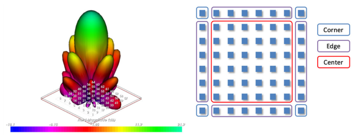
The radiation pattern of each antenna element will likely be affected by its position in the phased array. These patterns may be measured in the lab or calculated in AWR AXIEM or Analyst software. A simple approach to characterizing the appropriate radiation pattern for a given element is to use a 3X3 phased array and excite one element, either the internal element, one of the edge elements, or one of the corner elements, while terminating all others. This will provide the internal, edge, and corner element radiation patterns, which can then be automatically stored in data files using the AWR software output data file measurements (the same technique used in the example above). This approach includes the effect of mutual coupling from first-order neighbors. An array with a larger number of elements may be used to extend mutual coupling to first- and secondorder neighbors.
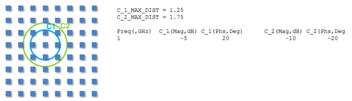
It is also important to capture the mutual coupling between neighboring elements. The AWR VSS phased array model does this through a coupling table defined in the configuration file. Different coupling levels can be defined based on distance from each other. The coupling, which is specified in magnitude (dB) and phase (degrees), is defined for two different distances (adjacent side elements: radius c_1 and adjacent corner elements: radius c_2) (Figure 11).
Modeling Impairments and Yield Analysis
RF hardware impairments of the array will affect the resulting side-lobe levels and beam patterns and will ultimately reduce system-level performance. For transmitter arrays, side-lobe levels from imperfectly formed beams may interfere with external devices or make the transmitter visible to countermeasures. In radar systems, side lobes may also cause a form of self-induced multipath, where multiple copies of the same radar signal arrive from different side lobe directions, which can exaggerate ground clutter and require expensive signal processing to remove. Therefore, it is critical to identify the source of such impairments, observe their impact on the array performance, and take steps to reduce or eliminate them.
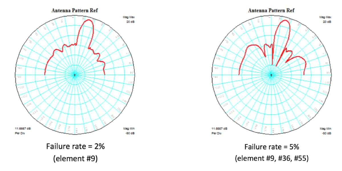
The AWR VSS phased array configuration file allows engineers to simulate array imperfections due to manufacturing flaws or element failure. All gain/phase calculations are performed internally and yield analysis can be applied to the block in order to evaluate sensitivity to variances of any of the defining phased array parameters. As an example, the AWR VSS software was used to perform an element failure analysis on a 64-element (16 x 4) array, producing the plots in Figure 12, which illustrates the side-lobe response degradation.
RF impairments also can be caused by any number of items relating to the feed network design and related components. Systematic errors that may be compensated include inter-chain variations caused by asymmetrical routing (layout), frequency dependencies, noise, temperature, and varied mismatching due to changing antenna impedance with steer angle, which also impacts amplifier compression. Therefore, it is imperative to be able to simulate the interactions between the antenna array and the individual RF links in the feed network.
RF Link Modeling
AWR software products include the simulation and modeling technology to capture these impairments accurately and incorporate the results into the AWR VSS phased array assembly model. This is an important functionality, since RF links are not ideal and can cause the array behavior to deviate significantly. The phased array assembly can operate in either the RX or TX mode, supporting the configuration of the array-element geometry, each element’s antenna characteristics, the RF link characteristics, and the common linear characteristics of the combiner/splitter used to join the elements together. The configuration is performed primarily through a text data file, with commonly swept settings either specified directly via block parameters (such as steering angles), or specified in the data file but capable of being overridden via block parameters (such as individual element gain and phase adjustments).
The configuration of the phased array assembly may be divided into several sections:
- Array geometry – Defines the number of elements, their placement, and any geometry-related gain and phase tapers
- Antenna characteristics – Defines antenna gain, internal loss, polarization loss, mismatch loss, and radiation patterns for both receive and transmit configurations
- RF link characteristics – Defines links for individual elements including gain, noise, and P1dB. Supports two-port RF nonlinear amplifiers using large-signal nonlinear characterization data typically consisting of rows of input power or voltage levels and corresponding output fundamental, harmonic, and/or intermodulation product levels. Frequency-dependent data is also supported
- Assignment of antenna and RF link characteristics to individual elements
- Power splitter characteristics – Splits the incoming signal into n-connected output ports
- Mutual coupling characteristics (previously discussed)
One common challenge is that not all RF links should be equal. For example, gain tapers are commonly used in phased arrays; however, when identical RF links are used for all antenna elements, elements with higher gains may operate well into compression while others operate in a purely linear region, causing undesired array performance. To avoid this problem, designers often use different RF link designs for different elements. While this is a more complicated task, AWR VSS phased array modeling enables them to achieve this, resulting in more efficient phased arrays.
To assist the design team creating the feed network and providing the RF link to the systems team, AWR VSS software includes the capability to automatically generate the characteristics of the phased array element link defined by the data tables. The designer starts by creating a schematic-based link design per the system requirements. A “measurement” extracts the design characteristics, which can include circuit-level design details (nonlinearities), through AWR Microwave Office co-simulation and saves a properly-formatted data file for use with the phased array assembly model.
In-Situ Nonlinear Simulations
An accurate simulation must also account for the interactions that occur between the antenna elements and the driving feed network. The problem for simulation software is that the antenna and the driving feed network influence each other. The antenna’s pattern is changed by setting the input power and relative phasing at its various ports. At the same time, the input impedances at the ports change with the antenna pattern. Since input impedance affects the performance of the nonlinear driving circuit, the changing antenna pattern affects overall system performance.
In this case, the input impedance of each element in the array must be characterized for all beam-steering positions. The array is only simulated once in the EM simulator. The resulting S-parameters are then used by the circuit simulator, which also includes the feed network and amplifiers. As the phase shifters are tuned over their values, the antenna’s beam is steered. At the same time, each amplifier sees the changing impedance at the antenna input to which it is attached, which affects the amplifier’s performance.
In this final example, the power amplifiers (PAs) are nonlinear, designed to operate at their 1db compression point (P1dB) for maximum efficiency. They are, therefore, sensitive to the changing load impedances presented by the array. The beam of a 16-element array is steered by controlling the relative phasing and attenuation to the various transmit modules (Figure 13). In practice, the AWR Microwave Office harmonic balance simulation used to characterize the power amplifiers takes substantial time to run with 16 PAs. Therefore, the beam is steered with the amplifiers turned off. The designer then turns on the individual PA for specific points of interest once the load impedance from the directed antenna has been obtained.
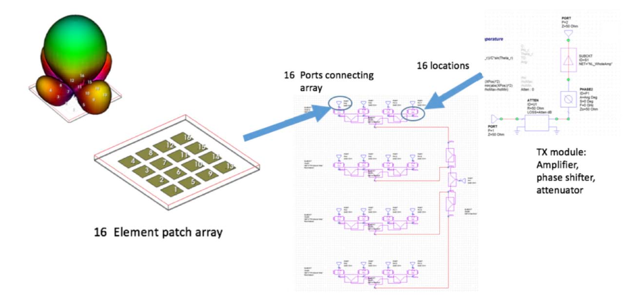
At this point the designer can directly explores the PA’s nonlinear behavior as a function of the load (antenna) impedance. With the load-pull capability in AWR Microwave Office software, PA designers can investigate output power, compression, and any other number of nonlinear metrics defining the amplifier’s behavior, as shown in Figure 14.
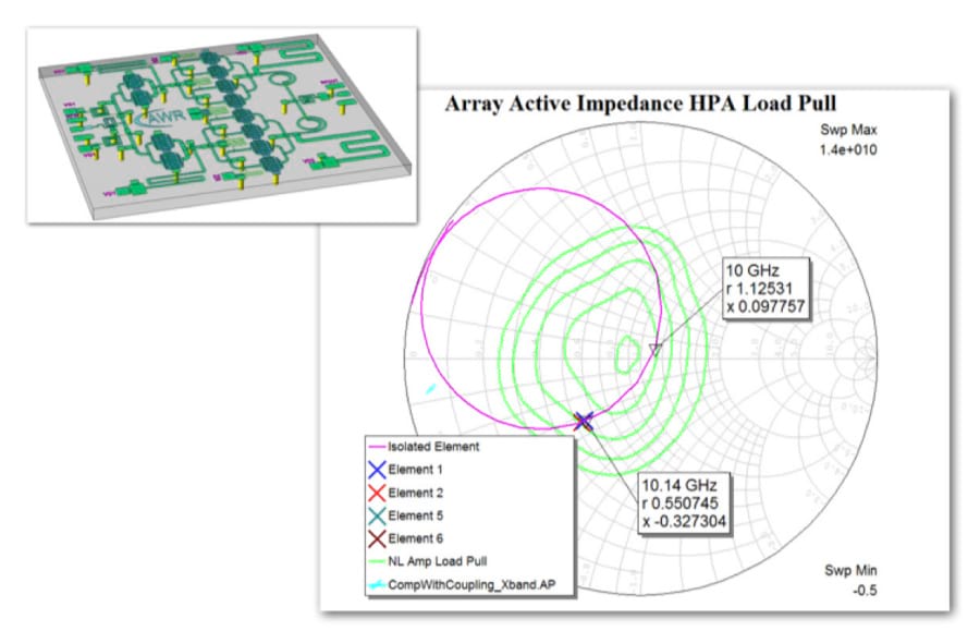
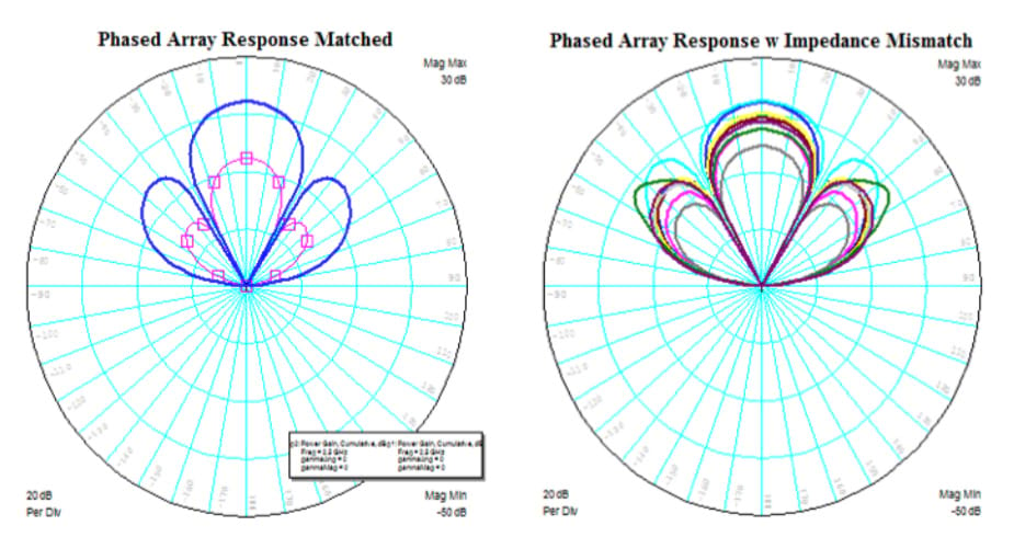
With a detailed characterization of the RF links for each individual element, the overall system simulation is able to indicate trouble areas that would have previously gone undetected until expensive prototypes were made and tested in the lab (Figure 15).
Conclusion
The capability to design and verify the performance of the individual components, along with the entire signal channel, is a necessity as element counts increase and antenna/electronics integration advances. Through a sophisticated design flow that encompasses circuit simulation, system-level behavioral modeling, and EM analysis operating within a single design platform, development teams can investigate system performance and component-to-component interaction prior to costly prototyping.
Acknowledgments
Special thanks to Dr. Gent Paparisto, Joel Kirshman, and David Vye for their contributions to this application note.