Application Note
AWR/Celsius In-Design Thermal Analysis Workflow: MMIC PA on PCB Example
The Cadence AWR Design Environment platform integrates electromagnetic (EM) and multiphysics analysis tools to support greater simulation accuracy and reduced development cycles for RF and microwave components and systems. Thermal analysis is now possible through the integration of the Cadence Celsius Thermal Solver within the AWR platform. This application note showcases the AWR/Celsius in-design thermal analysis workflow for a monolithic microwave IC (MMIC) power amplifier (PA) on a PCB.
Overview
Analysis Overview
Next-generation wireless communication and radar systems often demand more RF power within a smaller footprint to meet the performance and size requirements of their respective commercial and aerospace applications. Consequently, this exposes RF front-end electronics to the risk of higher operating temperatures, which degrade RF performance, and threatens device reliability. Thermal analysis provides RF circuit designers with insight into device operating temperatures that can be used by an electrothermal transistor model during simulation to generate more accurate RF simulations and guide the designer in developing more efficient heat mitigation solutions.
With the system trend to shrink footprints while integrating more electronics, the importance of EM and thermal analysis at the point of design has become critical to efficient and successful system development. Figure 1 illustrates how the AWR Design Environment Microwave Office circuit simulator and the Celsius Thermal Solver combine to provide insight into the operating temperatures across RF components and subsystems. The easy-to-use workflow takes advantage of AWR’s powerful extraction block technology to automatically generate a user-specified thermal structure complete with power dissipation information obtained from a Microwave Office harmonic balance (HB) circuit simulation of the structure to be analyzed, which can include a single transistor, entire MMIC (bare die or packaged), and/or PCB.
An MMIC PA on PCB Design Example
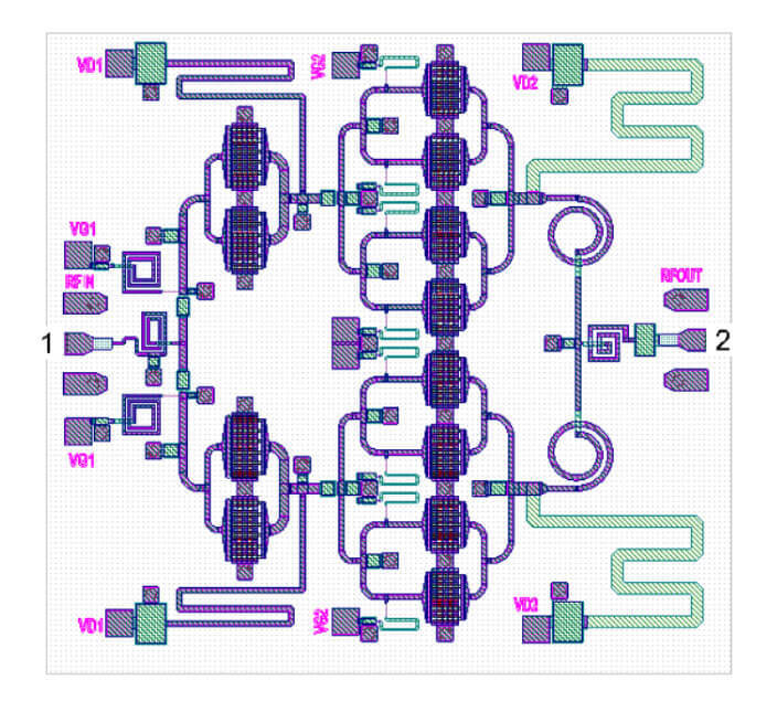
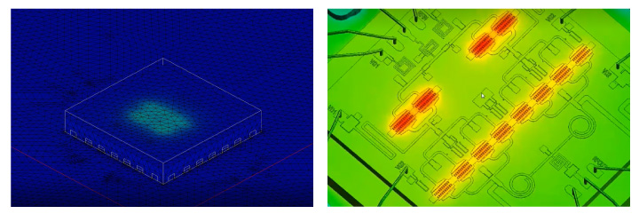
This example demonstrates the integration of the Celsius Thermal Solver within Microwave Office circuit design software for thermal analysis of a high-power X-band MMIC PA in a quad flat no-lead (QFN) bare die in package on a PCB. Figure 2 illustrates the thermal mapping results based on a hierarchical design, including a bare die, in-package, and mounted on a reference design PCB (test fixture). Scalable color mapping indicates the temperature gradient across the entire chip, package, and board.
Prior to design and analysis, a user-defined thermal layer with the prefix “Heat_” is added to the drawing layers in the project’s layout process file (LPF), providing a layer definition for all rendered heat sources. The footprint of the heat source can then be drawn on this layer during the model development/entry stage. For designs that include a transistor such as a MMIC, multiple heat sources can be defined within the transistor parameterized cell (PCell) itself, one for each channel of the transistor. In this case, the heat source is represented by a parameterized footprint that is coded into the PCell script by the foundry modeling team. Designers may also hand draw a heat source footprint on the design or within a component footprint, as might be the case for a packaged device. The CAD modeling team or the individual designer can address these steps.
Create Power Tables
First, the design is simulated using the APLAC HB circuit simulator in Microwave Office software to generate the power tables (Figure 3, bottom left), which the Celsius Thermal Solver uses to perform thermal analysis from power dissipation data. A new measurement type has been added to the most recent version of the Microwave Office software to create the power tables used for thermal analysis.
The power table is automatically stored as a data file within the project tree and lists all the elements in the circuit hierarchy that are dissipating power above a user-specified threshold value. This step occurs before defining the structures to be included in the thermal analysis.
Create EM Document
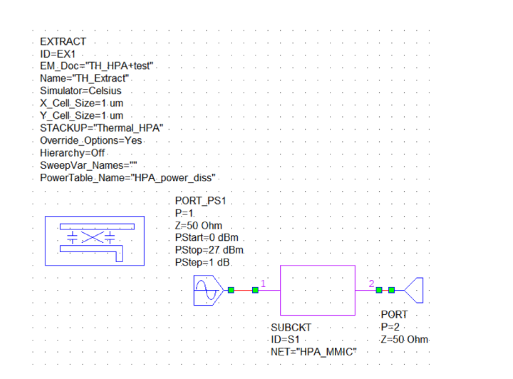
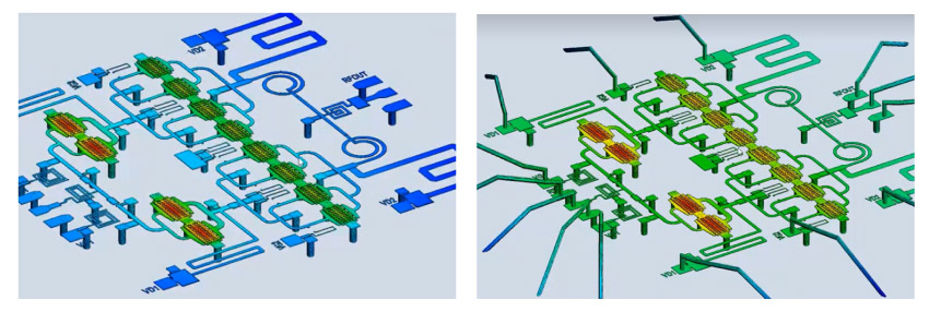
The next step is to create a thermal document that is identical to the method used for creating a standard EM document in the AWR project. The user places an EXTRACT block in the schematic and selects elements that will be incorporated into the EM/thermal subcircuit (document). Parameter settings in the EXTRACT block provide the stackup definition (EM and thermal layers), simulator to be used (in this case, Celsius Thermal Solver), and the name of the dissipated power data file, Figure 4. The user can generate the EM/thermal document for inspection by right-clicking the mouse on the EXTRACT block, or the block will automatically create this document when the user invokes a simulation. The power dissipation table “HPA_power_ diss” is associated with the MMIC die in the subcircuit, Figure 5. The design is now ready for thermal analysis of the bare die by itself. The next sections will discuss how the die was embedded into a package and mounted on a PCB for a more complete analysis of the die in its operating environment.
Place the IC in a Package
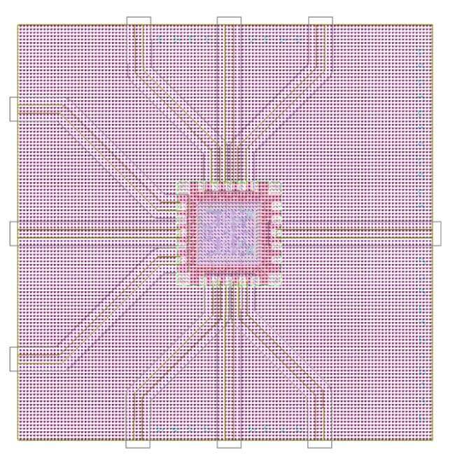
To capture the operating temperature of the MMIC device as it will be used in an application, the MMIC is placed inside a quad flat no-lead (QFN) package, taking advantage of the AWR Design Environment platform’s ability to support heterogeneous technologies within a single project. This example takes advantage of an existing 3D EM QFN package PCell that is available from the standard AWR 3D EM (package) library in the element browser (Figure 6).
Add the PCB Structure
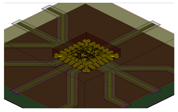
Finally, the PCB structure is added. Figure 7 provides a closeup of the die, bond wires, QFN package, and PCB. The full structure will be sent to the Celsius Thermal Solver.
The EM document options, available by right-clicking the mouse on the document in the project tree, allow the user to specify simulation settings that are passed along to the Celsius Thermal Solver, including the power dissipation table, temperature conditions, mesh settings, and settings for defining the solver’s behavior. The solver recreates the same 3D structure and assigns all the material properties to the different shapes inside the structure. It also brings across the power tables and associates them with the appropriate heat (elements dissipating power) sources.
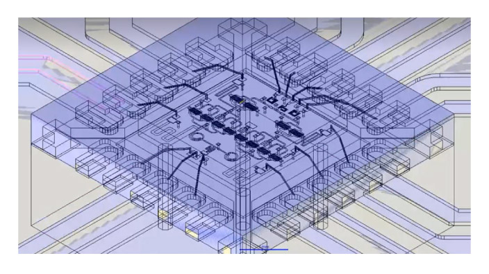
The Celsius analysis can take place directly within the AWR Design Environment without leaving the platform. The operating temperatures and thermal mapping are back-annotated to operating temperature tables, which link to the associated heat source for easy identification. Temperature color mapping is also back-annotated to the 3D viewer. Alternatively, the structure can be opened within the Celsius Thermal 3D workbench for inspection and analysis in the Celsius native editor, as shown in Figure 8.
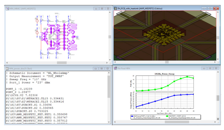
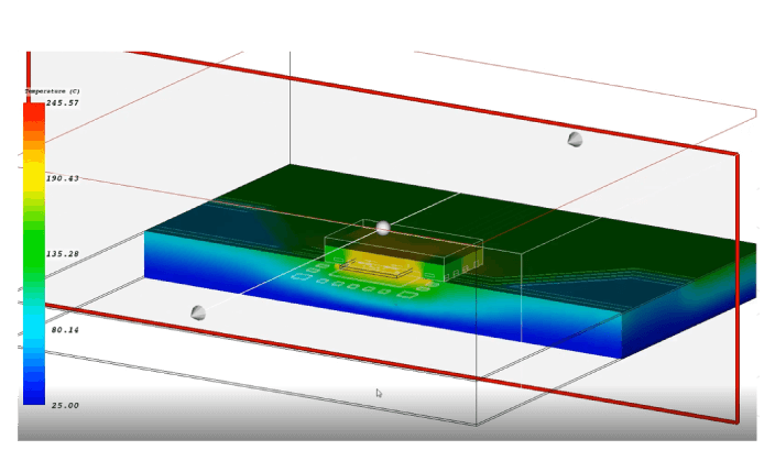
Once the simulation is completed, the full 3D structure can be viewed (Figure 9). The temperature (heat map) across the board can be seen on the left and the heat sources spread across the different power transistors of the MMIC on the right.
Single layers can be viewed by turning off the visibility of any of the layers. Figure 10 shows the die metalization on the left and the bondwires on the right.
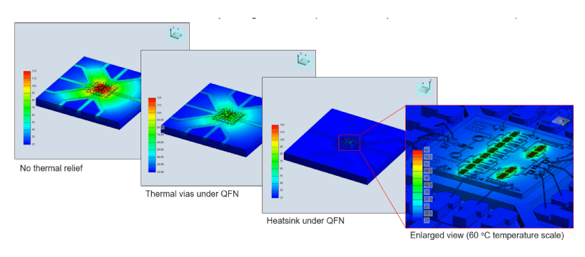
The scale for temperature distribution dynamically changes as more components are added. The cut setting can be selected to examine a slice, and the localized hotspots in the x, y, and z directions can be viewed (Figure 11).
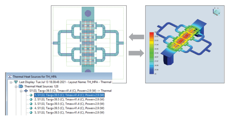
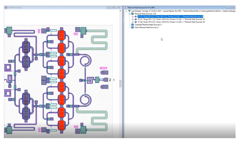
The Celsius Thermal Solver generates a results summary that is automatically sent back to the AWR environment as a data table listing the temperatures of all the defined heat sources, which in this example, includes the individual FET fingers. Users may select any entry from this summary listing, which highlights the heat sources of the individual components in red.
The average temperature across the power sources is 92.6°C, the maximum temperature is 92.5°C, and the power dissipation is 2.9W (Figure 12). With this junction temperature information, the designer can go back into the simulation schematic, assign the new temperature values to the devices, and rerun the HB simulation to generate a new power table. Those new powers can be sent back into the Celsius Thermal Solver, and a script is available to users that can run an iterative loop until the power dissipation vs. simulated operating temperature results converge.
Conclusion
This application note describes a new in-design thermal analysis between the AWR Design Environment platform and the Celsius Thermal Solver that enables RF designers to analyze the operating temperature for RF power applications and address thermal management concerns, including the package, PCB, and surrounding electronics. This flow, which has been illustrated using an MMIC HPA on a PCB example, enables the designer to perform more accurate simulations by incorporating heating effects and investigate heat mitigation strategies, thereby maximizing the performance of the PA by eliminating the need for a large thermal margin to be left on the table.