System-Driven PPA with Integrity 3D-IC Platform
Watch Now
Three-dimensional integrated circuit (3D-IC) is a die-stacking technology used in semiconductor packaging that offers new levels of efficiency, power, performance, and form-factor advantages to the semiconductor industry. 3D-IC is built by wafer-on-wafer or chip-on-wafer stacking on a single package interconnected using through-silicon vias (TSVs).
3D-ICs promise “more than Moore” integration by packing improved functionality into small form factors while enhancing performance and reducing costs. 3D-IC packages accommodate multiple heterogeneous die such as logic, memory, analog, RF, and micro-electrical mechanical systems (MEMS) at different advanced process nodes for high-speed logic and older nodes for analog. This provides an alternative to system-on-chip (SoC) integration, potentially postponing an expensive move to a new process node for all the functionality developers want to place in a single package.
SoCs today can pack increased functionality onto a single silicon die. SoCs typically include a processor, digital logic, memory, analog components, and embedded software. Some SoCs have hundreds of millions of gates and are pushing gigahertz speeds. The biggest concern with SoC design today is the rising development costs. Long development cycles also add to the costs.
The packaging options that have evolved over the years include package-in-package (PiP)—where several smaller systems in package (SiPs) may be mounted in a larger SiP—and package-on-package (PoP)—where one SiP may be mounted on top of another SiP. Both PiP and PoP assemblies may be categorized as 3D-ICs, but neither offers the performance, power, density, and form factor of true 3D-ICs using TSVs.
Until recently, silicon die has been attached to the SiP substrate using conventional wire bond and/or flip-chip technologies. Today, a silicon interposer substrate (either passive or active) may be added to provide much finer die-to-die interconnections, thereby increasing performance and reducing power consumption. A silicon interposer also includes TSVs, which connect the upper metal layers to additional backside metal layers. Sometimes this technique is referred to as 2.5D stacking.
3D-ICs with TSVs are expected to broadly impact networking, graphics, mobile communications, and computing, especially for applications that require small, ultra-light, low-power devices. Specific application areas include multi-core CPUs, GPUs, packet buffers/routers, smartphones, tablets, netbooks, cameras, DVD players, and set-top boxes.
3D-ICs with TSVs represent a significant new trend in the semiconductor industry. With the die-stacking option from different process nodes, the system components, including analog and RF, are no longer restricted to a single process node. Some significant advantages of 3D-ICs with TSVs, compared to traditional SoCs, can be summarized as follows:
Compared to a wire-bonded SiP, TSVs offer reduced RLC parasitics, better performance, more power savings, and a denser implementation. Compared to a silicon interposer approach, a vertical 3D die stack provides a higher level of integration, a smaller form factor, and a faster design cycle. But a 3D stack raises additional challenges, including thermal, timing, and power management concerns.
While there are no major showstoppers from a design or process point of view, much still needs to be done to bring 3D-ICs into volume production by mainstream users. New capabilities are required in system-level exploration, 3D floorplanning, implementation, extraction/analysis, testing, and IC/package co-design. A 3D-IC silicon realization flow will support unified design intent, abstraction, and convergence with physical and manufacturing data for optimal, timely, and cost-effective design. A well-defined ecosystem, including foundries, IP providers, EDA vendors, and OSATs, must emerge with design kits and reference flows.
Cost-effective 3D-IC design requires co-designing three fabrics – chip, package, and board. With comprehensive offerings in analog and digital implementation, packaging, and PCB design tools, Cadence is uniquely positioned to support the 3D IC revolution and provide the capabilities needed for the cost-effective design of 3D-ICs with TSVs.
The Cadence 3D-IC solution provides 3D design planning, implementation, and system analysis in a single, unified cockpit, addressing the requirements of 3D-IC design for digital SoCs, analog/mixed-signal designs, and entire systems. It enables hardware and software co-verification and full-system power analysis using emulation, prototyping, and chipset-based PHY IP for connectivity with power, performance, and area (PPA) optimized for latency, bandwidth, and power. The solution also offers co-design capabilities with custom analog design and board design, integrated circuit (IC) signoff extraction, static timing analysis (STA) and signoff with signal and power integrity (SI/PI), electromagnetic interference (EMI), and thermal analysis.
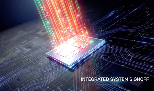
The Cadence Integrity 3D-IC Platform is a high-capacity, unified design and analysis platform for designing multiple chiplets. Built on the infrastructure of Cadence’s leading digital implementation solution, the Innovus Implementation System, the platform allows system-level designers to plan, implement, and analyze any stacked die system for various packaging styles (2.5D or 3D). Integrity 3D-IC is the industry’s first integrated system- and SoC-level solution that enables system analysis, including co-design, with Cadence’s Virtuoso and Allegro analog and package implementation environments.
Related Products
Related Articles