Clarity Electromagnetic Solver for Robust EM Simulation
Watch Now
Electromagnetic simulation is a modern method for analyzing the performance of electronic devices and systems using simulation and analysis software, which replaces costly and time-consuming legacy manual prototyping.
To accelerate the design process and meet aggressive delivery schedules, engineers need to be able to perform cross-fabric and multiphysics analysis to model, simulate, and analyze these effects on system-level designs.

There are two divisions or groups into which EM simulation software packages are divided: circuit simulators and field simulators. The software for EM field simulation is categorized according to frequency criteria, either low-frequency, which uses static electric and magnetic field simulation software, or high-frequency, which uses electromagnetic software. The more popular methods for field simulations now include the finite element method (FEM), boundary elements, or finite differences.
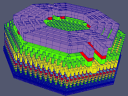
EM simulators first take in a physical description of the device, then process the layout into a form that can be used in the analysis phase. This typically involves “meshing” the conductors using the finite element method (FEM). The analysis is performed based on Maxwell’s equations for electromagnetism, and the solutions are combined to give a final result. The analysis result is provided as a model (such as S-parameters) that can be used in circuit simulation to verify performance.
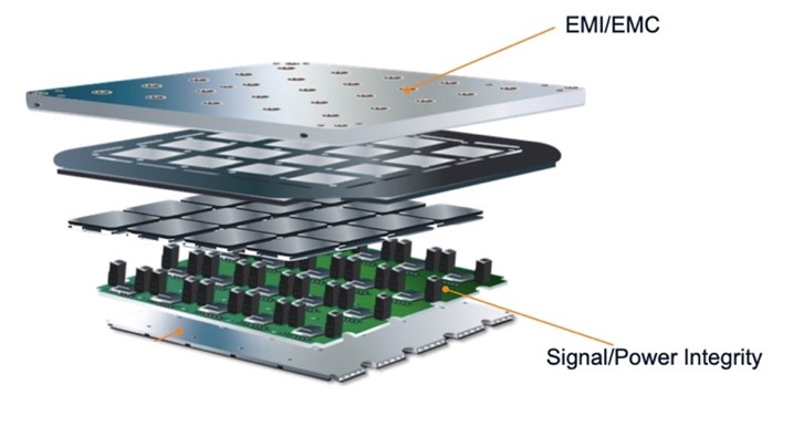
Today’s high-performance electronic systems are being driven by ever-increasing complexity and density, requiring designers to consider issues of electromagnetic interference (EMI) and electromagnetic compatibility (EMC), as well as power integrity (PI) and signal integrity (SI).
To accelerate the design process and meet aggressive delivery schedules, engineers need to be able to perform cross-fabric and multiphysics analysis to model, simulate, and analyze these effects on system-level designs.
The two main reasons for performing an EM simulation are to uncover any unintended EM interactions in the circuit/system and ensure the design meets performance specifications. In addition, there are different occasions on which a designer would want to perform EM simulation, such as when designing a chip, package, board, or system, to optimize the current design by looking at the results of the simulation and then tweaking it to improve it further. Alternatively, EM simulation is useful during the signoff phase, when the design is complete, and it is important to confirm that it is fully optimized and meets specifications.
Electronic product development projects have traditionally embraced a workflow in which the detailed multiphysics EM simulation, analysis, and optimization takes place at a very late stage in the design process, often as the final step of verification and signoff. However, this delay inevitably leads to costly issues that derail budgets and delay time to market as defects in requirements and performance are uncovered that require additional cycles to address these issues. These problems should have been discovered and mitigated earlier in the design phase.
To succeed in today’s highly competitive electronics markets, multiphysics EM simulation and analysis are now being integrated from the earliest stages of the design process in a methodology called “in-design analysis (IDA),” which is moving from an afterthought in the workflow to becoming an integral part of each phase of the design process at the chip, package, board, and complete system level.
An in-design workflow for RF/microwave devices provides EM optimization, parameterization, 3D EM libraries, circuit co-design, full-wave EM extraction, and multi-fabric EM hierarchy support. RF EM in-design technology allows design teams to transition from the ideal circuit design to physical designs with EM-level accuracy, building more complex circuits in a very logical and disciplined approach that helps the design team achieve their goals in the fastest time possible.
A 3D FEM solver can be used during the early stages of RF design, component EM modeling, circuit extraction, and optimization to uncover issues before they surface in the prototyping stage. These capabilities include 3D EM parameterized components and model libraries, support for hierarchical EM analysis of heterogenous designs, and EM extraction-on-demand features.
Every industry is expanding to embrace electrification, including mobile communications, aerospace/defense, industrial, biomedical, and consumer. Notably, modern automotive development is expanding to include more and more sophisticated electronics, and manufacturers are equipping their new models with advanced driver-assistance system (ADAS) applications to reduce injuries and fatalities by alerting drivers to and assisting them with a variety of issues, including collision avoidance and low tire pressure, as well as self-parking and driving. As demand for features increases, these systems become increasingly complex, making in-design EM simulation and analysis critical for delivering reliable and excellent performance within shrinking market windows.

In key electronics applications such as high-performance computing (HPC), automotive, machine learning, and 5G, data speeds and volume are increasing exponentially. Crosstalk analysis and simulation in high-speed design is difficult without the right field solver tools or analytical models. Designers of modern high-speed PCBs need to consider single-ended and differential crosstalk and power integrity problems that can be mistaken for crosstalk.
Designers need in-situ EM analysis to understand the relationship between physical design and overall system performance. In tandem with EM simulation and multiphysics analysis integrated within the design process, engineers also need solutions that enable complete and comprehensive high-speed and high-frequency design and analysis workflows within a single platform that goes beyond the chip and extends out through the entire system.
To address these requirements, EMI/EMC and SI/PI technologies can be used throughout the design process to quickly and accurately tackle the largest and most complex structures, identify sections of an interconnect that are susceptible to crosstalk, and take steps to prevent noise coupling between interconnects.
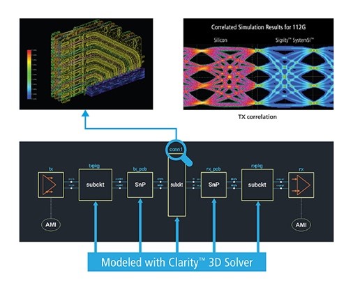
The Cadence Clarity™ 3D Solver provides optimum EM simulation and analysis for obtaining the high-speed/high-frequency electrical behavior of PCB, package, and IC structures using geometry and material information already defined within the Cadence Allegro® PCB or IC design and Virtuoso system design platforms. By offering EM analyses with virtually unlimited capacity that can cover the broad range of manufacturing technologies found in today’s heterogenous systems, designers can solve bigger problems without the added time, cost, and potential errors associated with design exporting, partitioning, simplification, and reassembly of analysis results. The Clarity true 3D EM field solver enables designers to avoid the error-prone divide-and-conquer methodology and simulate 10X faster while maintaining gold-standard accuracy.
Cadence Sigrity™ SI/PI technology delivers powerful, accurate planar 3D EM simulation of signal integrity (SI) and power integrity (PI) that addresses the size and scalability challenges of today’s leading-edge 5G communications, automotive, hyperscale computing, and aerospace and defense industries. The software works with all major PCB and IC package design platforms, including Cadence’s Allegro PCB, Allegro Package, and Integrity 3D-IC design platforms. It provides high-speed system designers with comprehensive, end-to-end SI/PI analysis, in-design interconnect modeling, and power delivery network (PDN) analysis for PCB and IC package designs. Working within a unified, integrated, and collaborative design environment, design engineers are more productive and able to meet compressed schedules and bring products to market on time and within budget.
The EMX Planar 3D Solver is an EM simulator for the design of high-frequency and high-speed ICs. It allows designers to accurately model complex layouts while reducing design cycle time. The solver is optimized for analyzing passives on silicon, primarily planar conductors and small vias like on-chip interconnect. It also has a broad library of process design kits (PDKs) from all the major foundries. This combination delivers quick and accurate processes. The EMX solver is seamlessly integrated with the Virtuoso platform and Virtuoso Studio.