White Paper
Power-Aware Analysis Solution
By reviewing the classic (or traditional) SI methodology, analyzing high-speed design flows, and examining what is employed in Cadence Sigrity power and signal simulations using the SPEED2000, PowerSI, Transistor-to-Behavioral Model Conversion (T2B), and SystemSI tools, this paper explains how a general power-aware SI solution not only should be capable of performing SSN simulations, but also capable of creating and extracting signal and power analysis-required models and running design checks with power-aware constraints. Providing such a complete, or true, “power-aware solution” gives designers the confidence to produce high-quality designs.
Overview
Introduction
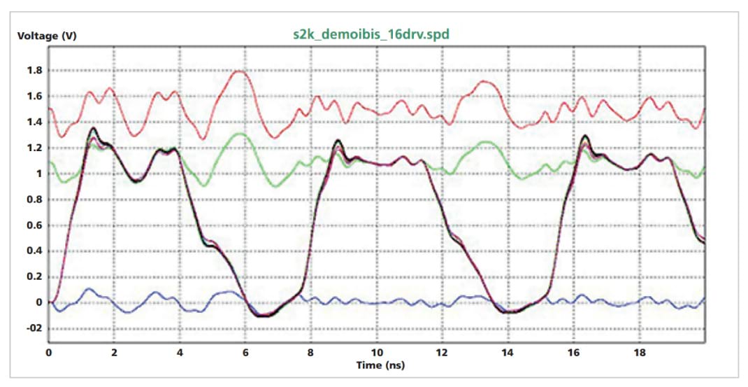
The term “power-aware” was first introduced several years ago. Since then, power-aware signal integrity (SI) has been used to refer to advanced SI simulation methodologies that can analyze signal and power noise simultaneously (Figure 1). These methodologies, however, are misunderstood by many people as the same simulation technology used to analyze simultaneous switching noise (SSN).
Is a power-aware solution just another fancy name for the method of simulating SSN? If it is not, what is the addition to make a power-aware solution? Are there technologies ready to provide a comprehensive poweraware SI solution?
Traditional SI Solution Review
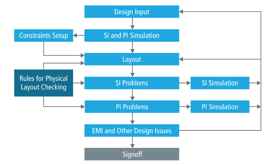
It is well known and understood by SI engineers that a traditional SI solution contains four parts: pre-layout exploration, constraint formation, rule checking, and post-route verification. Pre-layout exploration and post-route verification involve time and frequency domain simulation. The results help designers avoid signal degradation problems caused by interconnect effects such as delay, reflection, and crosstalk. Constraints and rule checking may involve little or no time/frequency domain simulation, but are derived from field solver results. In general, the constraints (DRC) are quick-checking rules and are implemented before or during the design, while rule checking in the post-route stage verifies the DRC implementation. The constraint-driven Allegro design flow was the first such solution in the industry. Today, many tools also use it as a “design-to-signoff” solution. Figure 2 shows a typical example flow.
One important fact people often forget about the traditional SI solution is that it was developed 20 years ago, and the data rates of high-speed digital designs have increased from 33MHz to over 4Gbps on parallel buses; not to mention that there was no serial link (with a data rate of a single channel today at 28Gbps or even higher) back then. Due to the lower signal speed of high-speed designs in the early days, the SI simulation and rule-checking methods used in the solution do not consider any power or ground net effects on signals. All the rules/constraints and simulations of reflections and crosstalk assume ideal power/ground planes as reference, without considering the interactions between power nets and signals. Correspondingly, the standard behavioral modeling approach for SI, IBIS, has no specification about current behavior through power supplies. The evidence can be seen in the early days of pre-layout tools—the device model symbols (driver and receiver) do not include any external power or ground connections.
Did the interaction between power supply and signals exist in the past? Yes, SSN has been seen with parallel bus design from the beginning, and SSN analysis is supposed to capture this phenomenon. Then why didn’t SI simulation tools include simulating SSN, instead of concentrating on delays, reflections, and crosstalk with ideal reference planes? The reason is simple: SSN analysis requires a significant amount of computing power and time, which the classic SI tool could not afford with less powerful computers. In addition, SSN analysis requires modeling a power/ground network that consists of planes, and classic SI tools did not have the right field solvers for this task.
Demands on Power-Aware Solutions
In the past 20 years, following the new design technologies (SerDes, DDRx) and the increased data rates, SI simulation advanced to include channel analysis for serial link designs, power integrity (PI) emerged to help design power delivery networks (PDNs) that provide stable supplies, and constraints/rule checking expanded rule sets to include constraints for SerDes and DDRx signals. Today, all major EDA tools offer classic SI analysis (delay, reflection, and crosstalk), DDRx analysis (DDR4 and LPDDR4 currently), channel analysis (SerDes), and PI analysis, with physical rule checking at certain levels.
As design margins become smaller and the number of power rails increases, the design industry has gradually realized that power and signal interactions often cause design failure. Unexpected power noise makes the timing and jitter budget inadequate. Designers need to know how much power noise may affect signal behavior by first looking for the tools that can simulate power and signal couplings. Further, they want to have the tools to help design power delivery and signals through the design cycle. This was clear at DesignCon 2016: high-speed designers asked EDA tools to simulate SI and PI together, to simulate chip, package, and board together, and to produce results in both frequency and time domains. These requests outline the direction of a power-aware simulation.
Definition of a Power-Aware Solution
What is the definition of a complete power-aware solution? In order to answer the question, let’s first take a look at how power and signal interaction affects SI.
-
 Reflection: Plane bouncing could couple to reflections from trace impedance-mismatch.
 - Crosstalk: Coupling between power supply net and trace generates new crosstalk, and crosstalk from trace coupling is also affected by plane bouncing.
- Timing: Due to the extra reflections and crosstalk caused by power noise, the timing margin also changes.
- Other:
- Signal via coupling through plane cavity has impact on reflection and trace crosstalk.
- Power switching noise couples to signal nets.
-
A power-aware SI solution must be aware of all these effects and be equipped with corresponding simulation and rule-checking techniques. These effects also show that SSN only represents some issues caused by signal and power interactions. SSN concentrates on multiple signal switching at the same time with a correct return current path. Power changes to affected signals are due to other output buffers’ drawing current.
An additional power-aware scenario occurs when plane noise caused by signal via coupling through the plane cavity is injected in to signals that are connected into the same supply as the parallel bus, but are not part of the multi-switching network that SSN analysis would focus on. The source of the noise can also come from voltage regulators on the PCB. Therefore, SSN simulation is only part of a power-aware solution.
A power-aware solution can only be implemented at the rule checking and post-route analysis stages because plane and signal interactions/couplings happen after routing is done. Therefore, a complete power-aware solution needs to provide:
- Time domain simulator capable of simulating large circuits (result of multiple signal and power nets)
- Power net and signal net modeling
- Advanced I/O buffer modeling
- Fast checking schemes for signal degradation and power effects on signals
Again, such a solution is not an equivalent definition of SSN analysis.
Power-Aware Solutions Available in Sigrity Technology
According to the definition given in the previous section, let’s now see if the Cadence toolset is ready to provide a power-aware solution.
For post-route SI verification, we have two approaches. The Sigrity SPEED2000 tool includes an engine with hybrid solvers that performs time domain simulation directly at the layout level and takes into account all couplings among signals, power nets, and vias. The Sigrity PowerSI tool has the same hybrid solver in frequency domain and can extract S-parameter models with a large number of signals and power nets coupled together. The Sigrity T2B tool provides functions to extract and build equivalent I/O buffer models from transistor-based buffer circuitry to allow current changes at power pins. And the Sigritry SystemSI tool connects all the models (I/Os, packages, and boards) to perform time domain simulation at the system level. The first approach blends the T2B I/O models with SPEED2000 simulation and performs the analysis directly at the layout level. The second approach takes the T2B I/O models and PowerSI S-parameter models and connects the models together in a block-level interface in the Sigrity SystemSI tool.
For rule checking, since constraints are formed at the early stage of a design with planes and vias not in place yet, whatever DRC rules implemented based on constraints are not power aware. When performing physical rule checking at the post-route stage, if done with the same method that generates constraints, no power noise effects can be captured. Therefore, any rule checking scheme or tool, based on an ideal plane assumption to check impedance, trace coupling, crosstalk, delay, or skew, will miss all power noise impact on signals. Using such a rulechecking tool (without considering the power noise effect on signals) for design signoff is dangerous, it means that the “signing off” is not finished yet because it does not, and cannot, identify the potential problems in a design caused by power and signal coupling.
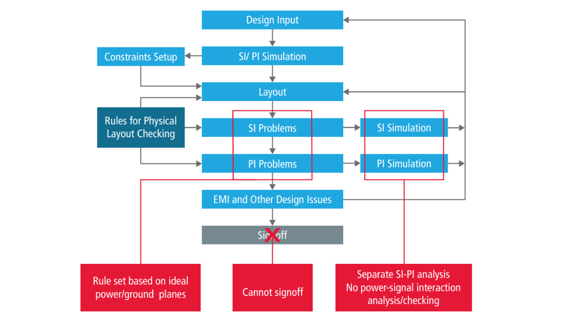
Figure 3 re-examines the signoff flow in Figure 2. It clearly shows that the solution only offers separate PI and SI simulations (no signal and power interaction), and that the rule set is derived based on the assumption of ideal planes. Therefore, users who employ this solution do not know if power noise will affect the signal’s quality or timing budget. The designs “signed off” by this solution may go out the door with design flaws and, even worse, without the designers’ awareness of those flaws!
What can we do to make the design checking also power aware? Since the power-aware requirement describes power and signal coupling, can we use a formula-based estimation to setup rules to check power and signal coupling? Because crosstalk estimation restricts the application to two parallel conductors only, it leaves estimating signal and power coupling out of the question. The reason is that the majority of power nets have large metal shapes, so there is no analytical solution to calculate the coupling between shapes and traces.
Does this mean we don’t need the rule checking and should rely solely on detailed/complex simulation? Not really. Before handing a design off for simulation, designers still need post-route checking, they need the checking to be power aware, and they need the results fast. Plus, designers are normally not SI/PI experts. It is difficult for them to run complex signal/power analysis and interpret results. What can be done then? The answer must be an efficient simulation method to identify problematic signals using pre-defined signal compliance.
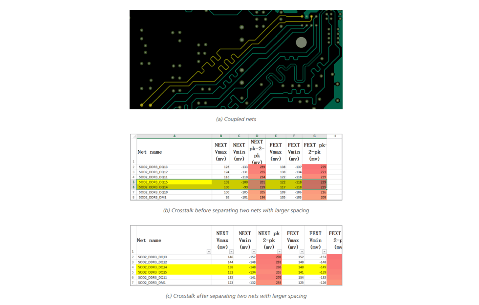
The quick-checking SI Metrics Check tool, offered in the SPEED2000 technology, performs analysis of signal and power coupling through linear excitations to a large number of signal nets. It reports signal quality with all coupling noise, while avoiding time-consuming non-linear simulation runs. The results of the SI Metrics Check guide designers to find issues that general post-route rule checking, assuming ideal reference planes, cannot find. Figure 4 shows such an example of using SI Metrics Check. Via coupling through plane can induce extra crosstalk and makes crosstalk increase with larger separation. The observation seems to violate the general crosstalk rule where crosstalk reduces as spacing increases, but it can happen on a real design due to via coupling, impedance mismatch, and plane noise. SI Metrics Check captures the problem in quick screening. However, it cannot be detected by physical rule checking tools.
The next question is what designers should do with the reports of SI Metrics Checking. The power-signal coupling issues identified, or the problems captured, by this checking can be fixed by making the plane “quieter”, i.e., to place the correct number of decoupling capacitors with correct values to the power supply nets to limit the power noise. This task needs a PI tool and capacitor optimization techniques. The PowerSI and OptimizePI technologies are the industry-leading tools for these purposes. After the PDN design is properly verified, i.e., power noise is minimized, planes are close to ideal reference and all rules with ideal reference plane assumptions can still be used.
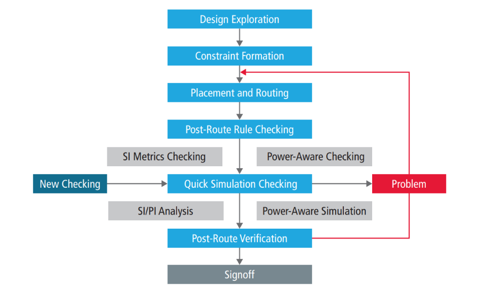
Figure 5 demonstrates the power-aware checking and simulation flow discussed above.
Conclusion
This paper discusses in detail how a power-aware solution should be defined and how it is different from SSN analysis. It points out the flaw of the “physical rule only checking”-based signoff solution and proves why the commonly used signoff solution is incomplete. It is important to remember that not all power-aware solutions from different tool providers are equal. When examining a power-aware solution, designers need to see if the solution contains the necessary capabilities we discussed earlier in the paper.
- Can the solution extract large network models of package/board with power and signal coupled together accurately and efficiently?
- Does the solution provide a tool to create or build advanced I/O models for power-aware analysis?
- Can the solution perform efficient electric checking on power noise effects on signals that geometry-based DRC cannot comprehend?
If these criteria are not satisfied, the solution is not truly power aware.
Further Information
Learn more about Cadence’s power-aware solutions at Power-Aware Signal Integrity Analysis.