Datasheet
Clarity 3D Solver for EM Analysis of RF/Microwave Systems
3D FEM EM design verification inside Microwave Office software
The Cadence Clarity 3D Solver electromagnetic (EM) simulator, used for designing critical interconnects, IC modules, PCBs, packaged acoustic filters, and system on ICs (SoICs), overcomes the limitations of legacy EM analysis software by leveraging Cadence distributed multiprocessing technology to deliver virtually unlimited capacity and 10X simulation speed improvements. This powerful 3D EM simulator based on highly accurate finite element methods (FEM) is now integrated within the Cadence AWR Design Environment platform, providing RFIC/monolithic microwave IC (MMIC), module, and RF PCB designers with ready access to high-capacity EM analysis for design verification and signoff of large, complex RF/ mixed-signal systems.
Overview
Analyze Large Complex RF Designs
Cadence developed the Clarity 3D Solver from the ground up to take advantage of multicore compute resources by simultaneously executing or parallelizing the mathematical tasks required to solve complete 3D structures, no design fracturing necessary. Industry-leading parallelization technology ensures that meshing and frequency sweeping can be partitioned and parallelized. The amount of time required to solve is scalable based on the number of computer cores. If a user can double the number of computer cores, the performance will be nearly doubled as well.
Product Strengths
3D Modeling
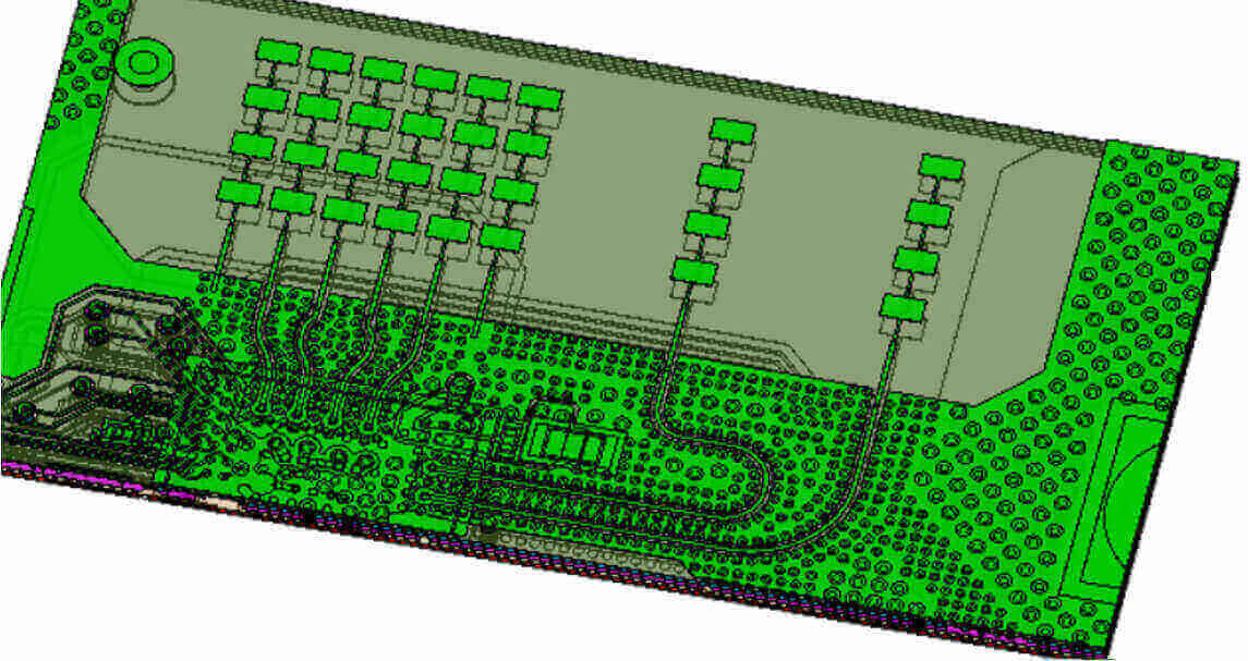
With the Clarity 3D Solver, you can readily characterize passive 3D structures, including distributed planar structures, interconnects such as vias, ball grids and bond wires, complex electronic packaging, and structures as a standalone design or directly within a circuit network. From within Cadence’s Microwave Office software, an EM document can be created directly from layout data or based on imported PCB and/or system-in-package (SiP) data from tools such as the Cadence Allegro environment (Figure 1). Seamless integration of the Clarity 3D Solver within the AWR Design Environment platform greatly reduces design time and increases design quality by eliminating manual steps and associated errors. Support for 3D CAD file formats like IGES, STEP, and STL allows designers to perform EM analysis on structures from a variety of mechanical CAD tools.
Creating 3D structures and launching a simulation in the Clarity 3D Solver is the same process as working with a Cadence Analyst FEM EM analysis document. The procedure for drawing finite dielectrics and resolving material priority with overlapped shapes is identical. Geometry simplification using shape pre-processing rules is further supported with both 3D FEM EM technologies, and a preview geometry feature can be used to visualize the simplified geometry in the Microwave Office software’s EM editor. In addition, the Clarity 3D Solver’s native editor can be launched directly from the Microwave Office software for viewing, validating, debugging, and post-processing of the geometry and simulation results.
Simulation and Design Exploration
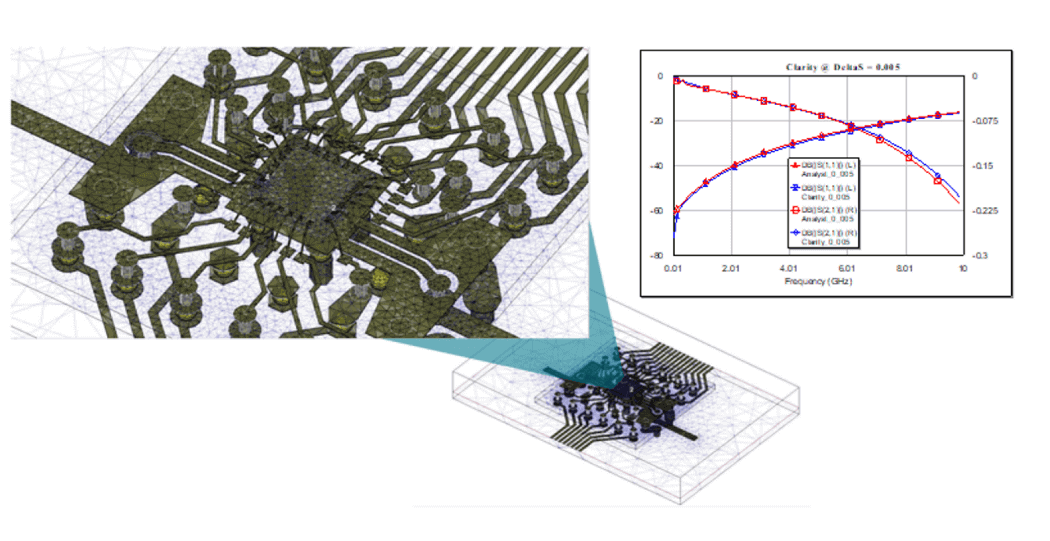
S-parameter results, mesh, original input geometry, translated geometry, and simulation logs from the Clarity 3D Solver are automatically returned to Microwave Office software, where simulation data sets are readily available for generating measurement graphs and tables. Performance is automatically improved, and design problems from unforeseen resonances and coupling between structures are mitigated with 3DEM parametric studies that support optimization, tuning, and yield analysis (Figure 2).
In-Situ Extraction
EM simulation with the Clarity 3D Solver is also supported through user-selected extraction of components and subcircuits within the Microwave Office software’s circuit schematic, resulting in a simulation-ready EM document with assigned excitation ports, material stackup, and boundary definitions. The workflow supports EM document hierarchy, allowing modelers to investigate EM effects (parasitic behaviors such as coupling and resonances) across heterogenous technologies.
Benefits
-
 Avoid costly implementations, engineering delays, product iterations, and field failures through simulation of potential design flaws
 - Eliminate late-stage design iterations by accurately predicting how a product will perform in the lab
- Improve efficiency and communication between RF/ microwave IC, packaging, and PCB design/analysis teams through shared models and simulation data
- Provide integrated model extraction capabilities for chip, package, and PCB designs to identify problems and avoid re-spins
- Accelerate product development with complex 3D EM structure modeling with near-linear scalability in speed and memory reduction
AWR Platform Features
RF/Microwave In-Design
The AWR Design Environment platform offers many powerful automation features for developing embedded RF/microwave circuits such as resonators, filters, and impedance matching networks in limitless manufacturing technologies. Concurrent schematic/layout design entry and user-selectable EM extraction from layout creates full-wave EM structures easily and on demand. Support for EM optimization, parameterization, and simulation-ready 3D EM libraries (wire bonds, connectors, etc.) allows designers to rapidly define their designs and optimize performance with the Clarity 3D Solver’s speed and accuracy. In addition, Microwave Office software supports multi-fabric EM hierarchy for analysis of integrated heterogeneous technologies.
Co-Simulation with Microwave Office Software
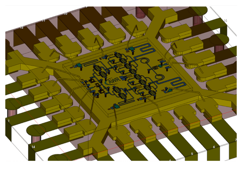
For RF/microwave circuit designers focused on module design and component integration, seamless circuit/EM co-simulation is enabled between Microwave Office circuit design software and the EM technologies of Cadence’s AXIEM 3D planar, Analyst 3D, and Clarity 3D Solver EM simulators. This streamlined and automated workflow allows Microwave Office software users to readily access the Clarity 3D Solver for S-parameter extraction and analysis of EM fields and currents of large and/or complex 3D-layered structures found within MMICs, densely populated RF PCBs, and multi-function RF/microwave modules (Figure 3).
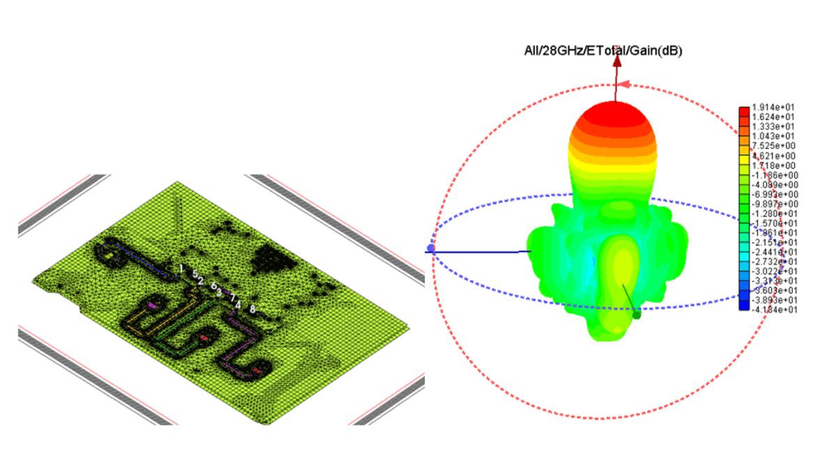
Antenna Design
Using the Clarity 3D Solver within the AWR Design Environment platform provides access to many rich features for antenna design and optimization, including antenna measurements for generating standard and custom response plots such as antenna gain, efficiency, return loss, radiation patterns, and more. Peak performance antenna measurements provide antenna metrics across frequency bands and other swept parameters. The phased array wizard in VSS software allows array designers to rapidly explore far-field performance versus user-defined array configurations using the Clarity 3D Solver’s generated radiation patterns and includes the impact of gain tapering, feed network and element links (phase and amplitude controls). The wizard can then generate a physical design using the original single element structure to populate an entire array for EM verification with the Clarity 3D Solver (Figure 4).