Brochure
112Gbps XSR SerDes IP for TSMC 7nm FinFET
Overview
Overview
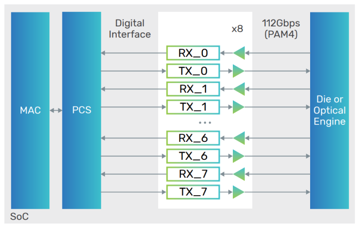
The Cadence 112Gbps Extra Short Reach (XSR) SerDes IP for TSMC 7nm consists of eight lanes operating at 112Gigabit per second using PAM4 modulation. This IP enables die-to-die or die-to-optical engine connectivities for extremely low power and compact footprint. 112G-XSR SerDes is an enabling technology for chiplet and systemin-package (SiP) applications, which allows SoC providers to deliver more customized solutions that offer higher performance and yields while also shortening development cycles and reducing costs through greater IP reuse.
The 112G-XSR SerDes IP supports primary Ethernet data rates within +/- 200ppm. Each receiver includes clock-data-recovery (CDR) for tracking PPM offset. An integrated micro-controller allows for fully autonomous startup, adaptation, and service operation without requiring ASIC intervention. A programming and observation interface is provided via a parallel bus with MDIO-style addressing (port, device, address).
There are several comprehensive on-chip diagnostic tools that enable testability and easy debugging. A post-equalized histogram is available for accurate estimation of bit error rate (BER) even in the absence of actual bit errors. Vertical eye statistics can be logged to allow optional optimization of the device settings. The Channel Estimator hardware allows the accurate measurement of the channel response to assess package, connector, and trace characteristics.
Benefits
-
 Small area and low power is ideal for System-inPackage (SiP) application
 - 1Tbps/mm beach front density
- Support north-south and east-west SOC edge placement
- Comprehensive on-chip diagnostic features make system testing/debugging quick and easy
Key Features
- TSMC 7nm FinFET CMOS Process
- 112G PAM4 interface compatible to LR and VSR
- Eight-lane compact footprint for high-density designs
- Integrated BIST capable of producing and checking PRBS
- OIF-CEI-112G-XSR standard compliance
- Power-optimized for XSR links
- Fully autonomous startup and adaptation without requiring ASIC intervention
Product Details
There are eight instances of the transmitter and the receiver in the IP.
Transmitter
The transmitter (TX) includes standard encoding, a DAC that converts digital signals to an analog output, with a digital FIR filter for waveform pre-emphasis. The transmitter drives a 100Ω differential output with adjustable swing.
Receiver
The receiver (RX) includes an analog front-end, a CTLE equalizer, and standard decoding.
Built-In Self Test (BIST)
The TX may be configured to transmit data from an internal PRBS generator using a list of selectable patterns. The RX may similarly be configured to deliver decoded bits to an internal self-synchronizing PRBS checker to count bit errors in the data stream. Received data may be looped back to the transmitter (see Figure 2).
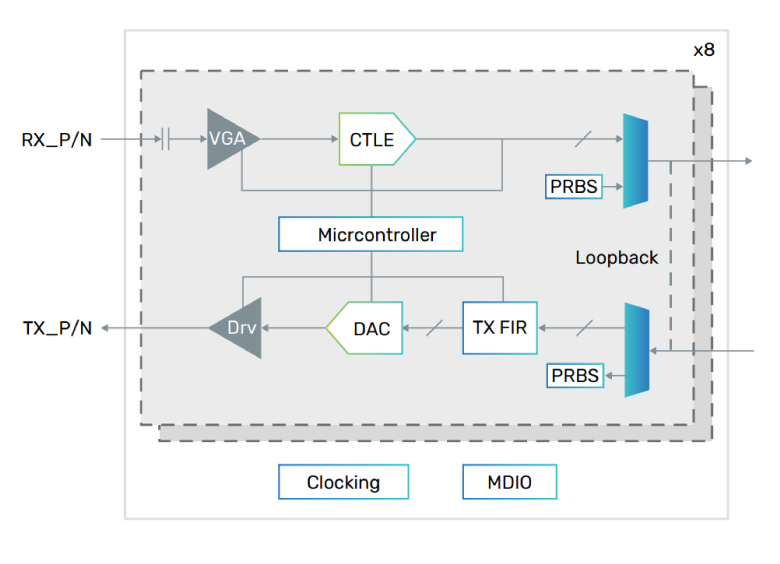
Clocking and Reference Clocks
All timing is derived from an external clock reference via an internal PLL and separate phase interpolators for the TX and RX lanes. The RX timing is locked to the incoming data, while the TX timing reference may be configured to derive either from the external reference, or optionally from the RX timing.
Deliverables
- GDS II macros with abstract in LEF
- Verilog post-layout netlist
- STA scripts for use at chip or standalone PHY levels
- Liberty timing model
- SDF for back-annotated timing verification
- Verilog models of I/O pads, and RTL for all PHY modules
- Verilog testbench with memory model, configuration files, and sample tests
- Documentation, including integration and user guide, release notes
- Verification IP setup files
For more information, visit Design IP.