White Paper
Interop Shift Left: Using Pre-Silicon Simulation for Emerging Standards
A CXL Case Study
The Compute Express Link (CXL) 2.0 specification, released in 2020, accompanies the latest PCI Express (PCIe) 5.0 specification to provide a path to high-bandwidth, cache-coherent, low-latency transport for many high-bandwidth applications such as artificial intelligence, machine learning, and hyperscale applications, with specific use cases in newer memory architectures such as disaggregated and persistent memories. In this paper, we describe how simulation interoperability (interop) between an Intel host and a Cadence IP has been key to the deployment of this emerging technology.
Overview
Introduction
New and evolving standards present unique challenges for interop as the ecosystem is nascent with limited opportunities available for interop testing. The addition of the CXL standard introduces cache coherency and low latency to what was a non-cache-coherent interconnect for PCIe, over the same PCIe PHY operating at Gen 5 and higher speeds. Interest in CXL is high, with over 160 member companies joining the CXL Consortium within two years of its formation. CXL is expected to enable usages from hardware accelerators to memory expansion in data centers to handle the growing demand for new compute workloads using the same hardware interfaces as PCIe.
The ecosystem is developing design IP, verification IP, protocol analyzers, and test equipment simultaneously, which could lead to possible issues not being discovered until prototype chips are available for interop testing, thus delaying product and solutions availability. Meanwhile, the CXL specifications are advancing to 2.0 and 3.0 revisions, and PCIe is extending to the 6.0 revision, with next-generation products rapidly entering the planning and development stages.
To keep up with the torrid pace of design innovations, there is a fundamental change in strategy to massively shift-left the verification of new CXL devices with the host IP. Intel and Cadence are working together on interop through co-simulation as the first proof point to successfully run complex cache coherent flows by first training the link using alternate protocol negotiation. The CXL simulation interop demonstrates the ability to confidently build host and device IP, while also providing essential feedback to the CXL standards body.
Verification Challenges
As with verification in any design process, the cost of finding an issue increases exponentially as we go through the various design stages.1
| Phase | Software Cost Factors | System Cost Factors |
|---|---|---|
| Requirements | 1X | 1X |
| Design | 5-7X | 3X-8X |
| Build | 10X-26X | 7X-16X |
| Test | 50X-177X | 21X-78X |
| Operations | 100X-1000X | 29X-1615X |
For advanced silicon geometries, such as 7nm, 5nm, Intel 3, and Intel 20A, the development time—from specification to architecture to implementation to verification to testchip tapeout to silicon characterization—can exceed a year. Silicon design costs for an initial design in 5nm compared to 7nm were projected to be 31% higher in 2019; software costs for advanced SoCs through the Intel 20A node era were forecasted to grow at 51% CAGR.2
Verification strategies for designs include unit/block-level testing, SoC-level testing, and system-level testing with directed and random tests along with formal verification strategies.3 With emerging standards, verification tools and infrastructure are developing concurrently with initial implementations—a challenge that IP developers are uniquely familiar with. CXL posed an even greater challenge due to the increased industry interest. Interop was key and it was paramount that Cadence’s solution be tested against the industry drivers so that broad market adopters could have confidence in the solution and the standard.
Cadence has a history of working with lead partners to perform silicon testing of our Controller IP solutions alongside industry-leading platform providers.4,5 Interop testing provides a measure of confidence beyond verification suites and compliance tests, which are limited in scope.
The challenge therefore is how to ensure interop at the earliest stage possible, before designs are released for production.
Interop Shift Left—Simulation
The most recent simulation interop, and the focus of this piece, is the Cadence Controller IP for CXL 2.0 Controller. A major challenge in developing the CXL 2.0 Controller IP, while the specification was evolving in 2020, was the lack of CXL 2.0 host platform availability for interop testing.
The CXL 2.0 protocol specifies that a CXL Endpoint must support both CXL 2.0 Endpoint discovery (like PCIe) and also be backward compatible to CXL 1.1 mode, whereby the Endpoint is discovered as a Root Complex Integrated Endpoint.
The solution was to partner with Intel for simulation interop testing with their future processor (CPU) designs that implement support for CXL. Through simulation, Intel had the opportunity to ensure backward compatibility against their existing CXL 1.1 solution and, in parallel, perform interop simulations on the evolving CXL 2.0 database (CXL 2.0 spec approved in October 2020).
This activity also benefitted the CXL developer community to have early adopters of the CXL standard interoperating with each other, with an opportunity to provide feedback to an evolving specification through errata discovery.
CXL Simulation Logistics
The CXL 2.0 protocol requires a CXL Endpoint to support both CXL 2.0 Endpoint discovery (like typical PCIe) and to be backward compatible to CXL 1.1 mode, whereby the Endpoint is discovered as a Root Complex Integrated Endpoint (RCiEP). The Cadence CXL controller and testbench application layer supported:
-
 PCIe and CXL modes of operation at 32GT/s rate of operation (PCIe 5.0 specification)
 - CXL v1.1 and v2.0
- CXL.io, CXL.mem, and CXL.cache
- 16 lanes
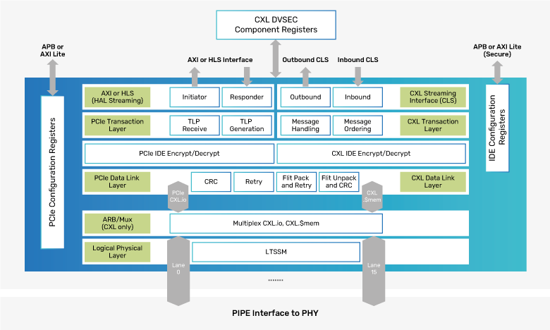
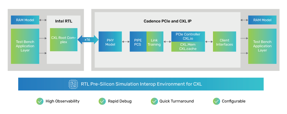
The Cadence CXL Endpoint RTL seamlessly dropped into Intel’s RTL simulation environment, replacing their Endpoint bus functional model (BFM).
A joint test plan was established to determine the area of testing, test strategy, and metrics to determine success. Test cases and traffic patterns included:
- CXL 1.1/2.0 link training
- CXL.io 1.1/2.0 discovery
- CXL.mem, CXL.cache, and mixed CXL.mem/CXL.cache traffic
- Traffic initiated by the host or Endpoint
Initial Interop
The Initial Cadence Endpoint Application Layer consisted of testbench style BFMs that responded to incoming requests and initiated outbound requests, via Verilog Tasks. The simplicity of the environment may be deceptive—it was highly capable and allowed us to achieve a number of our goals rapidly.
The first achievement, and not an insignificant one, was to train the link into CXL mode. A number of steps are required to successfully train the link and support exchange of transaction-layer messages:
- Creating the glue logic to connect the RP and EP controllers, via PIPE. Serial connectivity via a behavioral model of the PHY is supported in the controller RTL but was not used for this exercise as the CXL protocol test plan was independent of the underlying PHY. This was an acceptable tradeoff that could be made only in an RTL environment to rapidly achieve the overall protocol-level interop goals.
- Consolidating clock and reset architecture for the different implementations of RP and EP and achieving link training at each supported rate
- Interoperating with the newly defined CXL flavor of alternate protocol negotiation (APN) and modified training sequences
- Resolving operating modes, such as PCIe only or CXL with CXL.io, CXL.cache, and/or CXL.mem
- Performing dynamic rate change to 8, 16, or 32GT/s and achieving synchronization of newly defined CXL flow control units (flits) in the data stream
- Achieving interop of CXL-defined Skip Order Sets and Sync Header Bypass modes
- Performing CXL ARBMUX virtual link state machine (vLSM) state negotiation using ARB/MUX link management packets (ALMPs) to achieve Active state on all enabled CXL protocols
- Initializing the CXL.io data link-layer in flit mode
- Initializing the CXL.cache/mem link-layer, including exchanging CXL init.Param and credits
- Interoperating with CXL.cache/mem link-layer flit packing format, including a mix of formats
Application-Layer Enhancement
Building on the initial 16-lane 32 GT/s CXL link-up in CXL mode, the logical next step was to enable application capability. We replaced the BFMs with a reference CXL EP application layer, supporting a small memory application. This RTL-based application layer models a CXL Type3 device memory application.
Additionally, the application layer was the implementation of DVSEC, RCRB and port registers that typically lie outside an IP implementation. In this way, the CXL 1.1 host could discover and enumerate the application using a standard enumeration with real software sequences, such as those used in host platform BIOS firmware.
Benefits to Wider Community
The immediate benefits of this exercise helped improve design quality for the participants. Undertaking pre-silicon RTL interop accelerates the pace of verification at the early stages of development. Key learnings include:
- Designers can count on the full debug capabilities of a simulator, unlike silicon or FPGA environments. Tools such as RTL waveforms, assertions, coverage, and logfiles are easily available and facilitate problem resolution.
- RTL simulation is not limited by FPGA clocks speeds. We can simulate at PCIe 5.0 x16 speeds in simulation, which is not possible in current FPGA implementations without making design tradeoffs that would make the implementation very different from an SoC version.
However, there are also benefits to the wider community and ecosystem, as lessons learned from the interop were fed back into the CXL specification itself. Examples include:
- Generation of errata to evolving CXL standard, particularly where the standard was open to interpretation. For example, when CXL.io-only mode was negotiated, it may have been interpreted as bypassing ARBMUX.
- Interop work performed by adopters allows new and evolving sections of CXL standard to be pipe cleaned and confirmed before being fully published, such as combinations of ARB/MUX being exposed to recovery during initial link training.
- Synchronization on CXL 2.0 errata between vendors, where small clarifications had been added to the standard and missed by one vendor.
- Opportunity to learn from alternative interpretations of a standard, and support as alternate mode to increase interop robustness. For example, a requirement to retry after recovery, even during initial link training.
Third-party interop builds confidence in products, improving robustness of early-stage designs. Using the design in a different environment pushes the boundaries of assumptions made during initial development and exposes the nascent design to new types of stress. This improves released product quality for the customer base.
Conclusion
In order for such a model of interop to work successfully, the ecosystem—standards bodies, host/device silicon providers, software (OS/tools) providers, etc.—must collaborate at an early stage with a high degree of trust and confidence. Appropriate encryption tools allow IP protection and hardware-enhanced security. Dependence on software tool versions must be minimized to allow for the tactical parts of these exercises to be seamless. A common test plan needs to be established with appropriate resources invested on both sides for the best outcome. This pilot project exceeded our expectations, and we intend to pursue similar interop projects for future standards.
References
- Stecklein, Jonette M., et al, “Error Cost Escalation Through the Project Life Cycle” INCOSE 14th Annual Symposium, 2004
- Semico Research and Consulting Group, “Average Silicon Design Cost for SoCs Across All Geometries Was $4.8M in 2019” (retrieved August 1, 2021)
- Hendry, Hamish, Sakthivel Ramaiah, Derek McAulay, Gary Dick, “Accelerate Adoption of High-Speed, Low-Latency, Cache-Coherent Standards Using Formal Verification”, Cadence white paper, May 2021
- Cadence, “Mellanox and Cadence Demonstrate PCI Express 4.0 Multi-Lane PHY IP Interoperability”, news release, March 15, 2016
- Cadence, “Cadence Subsystem for PCIe 5.0 – Silicon Demo”, video, April 6, 2021