White Paper
3D-IC Design Challenges and Requirements
As demands accelerate for increasing density, higher bandwidths, and lower power, many IC design and packaging teams are taking a close look at vertical stacking multiple chips and chiplets. This technology, called 3D-IC, promises many advantages over traditional single-die planar designs. Some are using the term “More-than-Moore” to describe the potential of this new technology. Integration by stacking die and using advanced packaging technologies allows designers to cram more functionality into much smaller form factors, while improving performance and reducing costs. 3D-IC architectures can integrate multiple homogenous and heterogeneous die/chiplets, such as logic, memory, analog, and RF, into a single design. This provides an alternative to monolithic system-on-chip (SoC) integration, potentially bypassing the expensive move to a new process node for all of the functionality designers want to place in a single design. With comprehensive offerings in analog and digital implementation, packaging, and PCB design tools, Cadence is uniquely positioned to support the 3D-IC revolution and to provide the capabilities that are needed for cost-effective design of 3D-ICs
Overview
Introduction
3D-ICs are expected to have a broad impact in areas such as networking, graphics, AI/ML, and high-performance computing, especially for applications that require ultra-high-performance, low-power devices. Specific application areas include multi-core CPUs, GPUs, packet buffers/routers, smart phones, and AI/ML applications.
While there is great interest in this emerging technology, it is still in its early phases. Standard definitions are lacking, the supply chain ecosystem is still in flux, and design, analysis, verification, and test challenges need to be resolved. This paper presents a brief overview of 3D-IC technology, and then discusses design challenges, ecosystem requirements, and needed solutions. While various types of multi-die packages have been available for many years, this paper focuses on 3D integration and packaging of multiple stacked dies.
From a design standpoint, some retooling will likely be required for true 3D integration. Improved capabilities are needed in architectural analysis, thermal analysis, cross-die placement, timing, test, and verification. Additionally, new system-level functionality such as top-level planning and optimization, chip(let)-to-chip(let) signal integrity and IC/package co-design will be required. Some of these capabilities are available today and can be leveraged from the system design tools.
Ultimately, designers need a solution that can aggregate all the required functionality into a single design platform. A successful 3D-IC design environment will capture the top-level design intent up front, support abstraction with early estimation of power/thermal, and achieve convergence through implementation, extraction, timing closure, test, analysis, and packaging.
A Closer Look at 3D-ICs
SoCs today pack an incredible amount of functionality onto a single silicon die. SoCs typically include a processor, digital logic, memory, and analog components, along with embedded software. Many SoCs have hundreds of millions of gates and are pushing gigahertz speeds.
Perhaps the biggest concern with SoC design today is the rising development costs. According to industry estimates, SoC hardware and software development may top $500 million at the 5nm process node. Additionally, long development cycles result in additional costs. If costs cannot be reduced, advanced-node SoCs may only be feasible only for a small number of high-volume applications.
Additionally, traditional single-die SoCs have some inherent disadvantages. One is that all components are placed on the same die at the same process node, even though analog and RF design at advanced process nodes can be extremely challenging. If a design team tries to implement analog circuitry at an advanced process node, it may take a great deal of time to develop and test the necessary IP blocks, as well as cope with process-related issues, such as variability and leakage.
Another challenge for single-die SoCs is mixed-signal integration and verification. Placing analog and digital circuitry in close proximity can cause many problems. Alternatively, sensitive analog or noisy digital components could be placed in a separate IC, but that makes it necessary to drive signals between individual packages, which consumes power and reduces performance.
Finally, state-of-the-art SoC designs are reaching the physical size limitations (reticle size) of what can be manufactured. Of course, these near reticle limit-sized devices typically don’t yield very well.
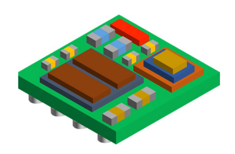
One long-standing alternative to the single-die SoC approach is to place multiple bare die into a single package. This makes it possible, for example, to use a 28nm process for analog/RF circuitry, and a 10nm process for digital logic. The terms systemin-package (SiP) (Figure 1), and multi-chip module (MCM) have all been used to refer to these technologies where multiple die are mounted on a common laminate substrate that is used to connect them together. These technologies have been used as early as the 1980s.
The SiP approach offers several advantages compared to SoC implementations, including the fact that the various analog, digital, and memory dies can each be implemented using the most appropriate technology process for that domain. In addition to logic, memory, analog, and RF functionality, modern SiPs may also include micro-electromechanical systems (MEMS) components, such as antennas or mirrors.
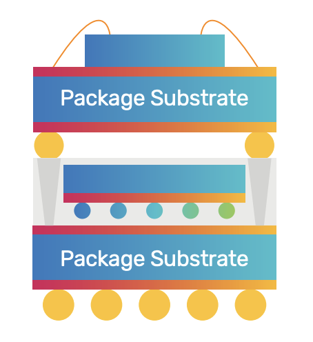
Another packaging option that has evolved over the years is package-on-package (PoP) (Figure 2), where one package may be directly mounted on top of another package connected with through molding vias. PoP assemblies may be categorized as 3D packaging, but this solution doesn’t offer the performance, power, density, and form factor of true 3D-ICs.
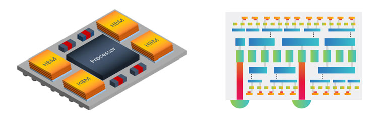
One of the latest evolving 3D packaging technologies is silicon interposers with through-silicon vias (TSV) that provide direct connections from top metal layers to the back-side metal layers. These interposers provide another level of package integration between the die and the laminate package substrate and provide much finer die-to-die interconnections. This results in increased performance and reduced power consumption. This technology is typically referred to as 2.5D-IC design. Some designers lump this technology under the term 3D-IC. Compared to a wire-bonded SiP, TSVs offer reduced RLC parasitics, better performance, more power savings, and a denser implementation. Compared to a silicon interposer approach, a vertical 3D die stack using hybrid bonding can offer an even higher level of integration, smaller form factor, and faster design cycle (Figure 3) . This paper primarily discusses 3D integration, although design methodologies developed for 3D-IC would lend themselves quite well to the design of 2.5-IC silicon interposers.
The advantages of 3D-ICs, compared to traditional SoCs, can be summarized as follows:
-
 Lower costs are possible, because all functionality, including analog and memory, does not need to move to advanced process nodes.
 - It’s easier to meet high interconnect speeds and bandwidth requirements, which will reach >200Gbps for advanced memory technologies and SerDes.
- 3D-ICs allow miniaturization, saving space on the board and in the end-product. They can be ideal for extremely compact mobile devices.
- 3D-ICs can reduce power because big drivers are no longer needed. A 3D stack can use small I/O drivers with lower power. Further, reduced resistance-inductance-capacitance (RLC) helps reduce power.
- Interconnect between packages is reduced, allowing for faster performance and a better power profile.
- Time to market can be faster, thanks to modularity, the potential for “IP reuse,” and the ability to leave analog/ RF at higher process nodes.
- Emerging technologies such as photonics or MEMS can potentially be integrated into 3D stacks.
3D-IC Design Challenges and Requirements
Although several point tools are available today to design a 3D-IC, it’s up to each design team to develop their own methodologies to integrate the flow. This makes designing a 3D-IC today quite a challenge. Design teams are forced to spend more time writing scripts and customizing the design flow for each design and less time on actually doing design work. Many compromises are made in the process. The four big challenges that arise when pivoting from a single SoC to a multi-chip(let) architecture are as follows:
- Top-level/system-level heterogenous design aggregation, planning, and optimization
- Co-design and co-analysis of the die, chiplets, packaging, and PCB across digital, analog, and RF domains
- Early pre-layout thermal analysis
- A common platform that seamlessly integrates these technologies together
Let’s start with top-level planning. Here, it requires a solution that allows cross-domain design teams to enter abstract design representations into a single view. The ultimate goal of this solution is to create a fully optimized netlist from chip(let)-tochip(let) to packaging and even to the PCB. This netlist will be required to validate connectivity of the system-level design during signoff. This database must be 3D-aware and allow the design team to derive the optimal 3D stack of chip(lets). Optimization of the design should be based on early thermal and power analysis results as well as routability (reduced wire length) and ideally managing clock skew across the design levels. 3D-IC architectures typically require substrate thinning, resulting in relatively poor heat dissipation across the 3D stack. This makes accurate thermal analysis and signoff a critical step in the design flow.
Developers of 3D-ICs need to remember that any electronic product includes three different levels of interconnect—chips, packages, and boards. Designing the chip first and throwing it “over the wall” to package and board designers will not result in design convergence on an optimal, cost-effective solution. As mentioned earlier in this paper, 3D-IC design is a shared effort across multiple domains. The package designer knows how they want to optimized pin assignments for routability, but typically, knows little about the design of the IC. The IC designer can put micro-bumps inside the die, but has limited knowledge of how this impacts the package layout. The PCB designer will have to integrate the package with other components on the board. 3D-ICs will require close collaboration and co-design among groups that have historically worked separately. The ideal 3D-IC design platform must support robust co-design across all design domains. If the chip, package, and board are not designed cooperatively, the interconnect will not be optimized, and extra vias will be needed to handle signals that cross from one point to another. Consequently, performance will be reduced, additional board layers may be needed, and board and package costs may rise. Further, without co-design, timing, power, and signal integrity will not be optimized.
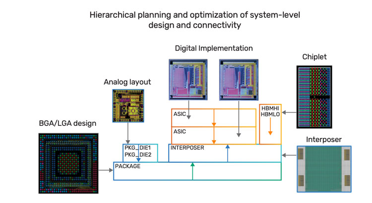
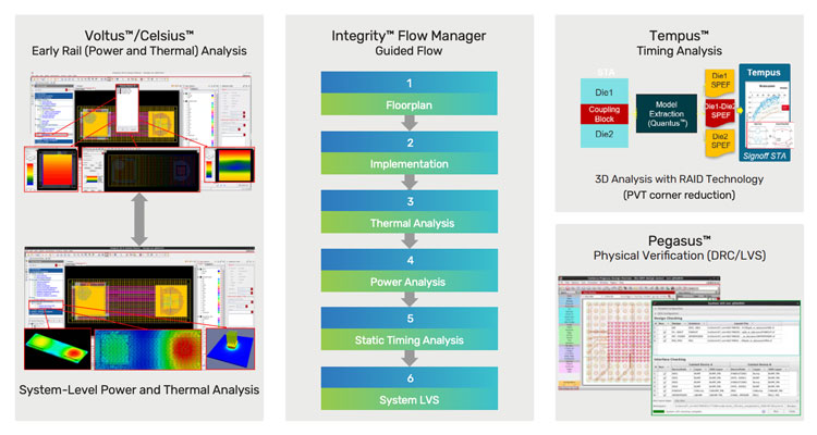
Finally, the ideal 3D-IC design platform should provide the end-user with a single cockpit design experience. This means that all of the point tools for planning, co-design, analysis, and signoff should be able to be directly set up and run from this design platform (Figure 4).
Extraction and Analysis
Extraction and analysis tools are crucial for design convergence. However, existing extraction and analysis tools need to be extended for 3D-ICs. For example, the tools must consider layout parasitics for TSVs, micro-bumps, and interposer routing. Further, analysis tools must be 3D-aware. Timing, signal integrity, power, and thermal gradients must be analyzed across multiple chip(let)s and into the system-level design. The multi-chiplet design must be validated using static timing analysis (STA) and with an understanding of interactions between multiple chip(let)s and the package. In addition, because moving to multi-chip(let) 3D architectures dramatically increases the number of corners to close on timing, a new STA solution with corner reduction is mandatory.
Electromagnetic interference (EMI) is a likely concern for 3D-ICs, raising a potential need for analysis tools. A multi-die package offers less shielding than a single-die package, and thus, offers more likelihood that emissions could escape. Here again, a seamless integrated solution for multi-chip(let) 3D design is critical to the success of the end-product.
Physical verification raises new questions with 3D stacks. For example, how can design rule checking (DRC) and layoutversus- schematics (LVS) run on the entire system-level design? Can timing be verified for the entire stack? Is there any crosstalk between dies?
Finally, to facilitate TSV connections, the wafer is thinned to implement a 3D-IC. This causes stress and adds susceptibility to thermal changes. Testing and checking for CMP planarity is needed across a range of thermal variations to ensure the wafer won’t warp, bend, crack, or break. (Figure 5)
Design for Test
Testing raises many challenges for 3D-ICs, including access to chip(let) inside a stack, and proper handling of thinned wafers. Thankfully, there are emerging standards for the 3D-IC test. Ensure that the tool you’re using for DFT meets all of the latest standards. Like conventional single-die IC test, the 3D-IC test must be considered at two levels—wafer test (for the bare die), and package test (after assembly and packaging). The difference is that there are many more intermediate steps in 3D-IC fabrication, such as die stacking and TSV bonding. This provides many more opportunities for the wafer test before final assembly and packaging.
Wafer test is needed for cost optimization. If a die is bad, it can be thrown away before it is placed in a package. If a packagelevel test fails, the entire package would have to be thrown away. Thus, the wafer test is highly desirable, especially early in the product lifecycle, while defects may still be relatively high.
Wafer-level test for 3D-ICs can be challenging for three reasons. First, some probe technology is unable to handle the finer pitch and dimensions of TSV tips, and is generally limited to handling several hundred probes, whereas the TSVs may have several thousand probes. Second, probe technology leaves scrub marks that can potentially cause problems with the downstream bonding step. Finally, the wafer test requires the creation of a known-good die (KGD) stack. To stack KGD, the wafer must be thinned by about 75% so that the tips of the TSVs can be exposed. However, as the thinned wafer is contacted by a wafer probe, there is a danger of damaging the wafer.
3D-ICs also introduce new intra-die defects. These may be introduced by new manufacturing steps, such as wafer thinning, or by bonding the top of a TSV to another wafer. Thermal effects are another potential source of defects because excessive heat may be generated from the densely packed stack of dies. Thermo-mechanical stress is caused by different thermal coefficients of the various materials in the stack. Despite the differences in the manufacturing steps, the resulting faults (shorts, opens, delay defects) appear similar to what we see in conventional ICs. It is possible that new fault models may be required, as we get more empirical data.
Modeling defects through TSV-based interconnects is a newer area. Defects may be introduced in the fabrication or the bonding of TSVs. Fortunately, defects introduced through TSVs can be mapped to existing fault models, such as opens, shorts, static, delay, and bridging faults. However, a methodology is needed to map TSV defects to known fault types.
A sound methodology for 3D-IC test should include a DFT architecture that provides efficient ways to control and observe individual die from the chip I/Os, while providing different test access modes (such as a mode for a KGD test or a known good stack test). Conventional DFT architectural approaches and techniques such as on-chip compression, boundary scan, memory built-in self-test (MBIST), reduced pin count testing, and on-chip clocking for at-speed test are broadly applicable and need to be configured and optimized to meet 3D controllability and observability goals. The trick is one of making an intelligent allocation of DFT resources across multiple chip(let)s to minimize the area overhead, while meeting constraints for test cost and shipped product quality.
Forging a 3D-IC Ecosystem
3D-IC may never become “mainstream” and step outside the IDM world unless 3D-ICs can be designed and produced in a cost-effective way, with sufficient turnaround time to meet market windows. This will be possible only with a robust and well-defined supply chain ecosystem, including semiconductor design companies, EDA vendors, IP suppliers, foundries, and outsourced semiconductor assembly and test (OSAT) providers. In many ways, the OSATs may have an advantage over the foundries based on their past work on SiP designs, where wafers from multiple foundries and substrates from across the globe have already been pulled together.
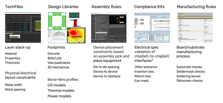
Foundries need to continue establishing design rules, create models and libraries, and provide process design kits (PDKs) and reference flows for 3D-IC. However, they might need to extend their role by starting to provide assembly design kits (ADKs) that extend coverage beyond 3D integration and into 3D packaging (Figure 6). The “A” in ADK stands for assembly, which is a key component to enabling design teams to move into the world of 3D-IC. Assembly rules would typically be based on the pick and place equipment that will automate the assembly of the 3D-IC design. Other components of an ADK would be system-level libraries and models as well as compliance kits to electrically validate chiplet-to-chiplet interfaces.
Conclusion
3D-ICs represent a major new trend in the semiconductor industry. They offer compelling power, performance, and form factor advantages in many application spaces, and they may curb the escalating costs of SoC development. Because designers can stack die from different process nodes, it is no longer necessary to move all system components, including analog and RF, to a single process node.
While the challenges of design flows are being sorted through, much remains to be done to bring 3D-ICs into volume production by mainstream users. New capabilities are needed in such areas as system-level exploration, 3D floorplanning, implementation, extraction/analysis, test, and IC/package co-design. For optimal, timely, cost-effective design, a 3D-IC flow will support unified design intent, abstraction, and convergence with physical and manufacturing data. A well-defined ecosystem including foundries, IP providers, EDA vendors, and OSATs needs to emerge, with design kits and reference flows.
Cost-effective 3D-IC design requires the co-design of three domains—chip, package, and board. With comprehensive offerings in analog and digital implementation, packaging, and PCB design tools, Cadence is uniquely positioned to support the 3D-IC revolution and to provide the capabilities that are needed for cost-effective design of 3D-ICs.