Technical Brief
RF/Microwave Design Software
Cadence AWR Design Environment, Version 15
Overview
Introduction
To meet the demand for increased data rates and capacity, communications, aerospace/defense, and automotive applications are utilizing more bandwidth, millimeter-wave (mmWave) spectrum, and spatial efficiency vis-a-vis multiple-in-multiple-out (MIMO) and beam steering phased arrays. Along with a need for small form-factor, cost-sensitive devices, RF to mmWave front-end components continue to evolve in order to keep pace with these new system requirements, the demands of enabling technologies, and space/cost considerations.
Engineering teams addressing these performance, integration, and cost/space goals face time-to-market pressures while striving to meet these increasingly complex product requirements. Engineers trying to bring these products to market need best-in-class simulation technology and design automation to accurately predict the performance of larger, densely integrated circuits/ subsystems designed for broadband and mmWave
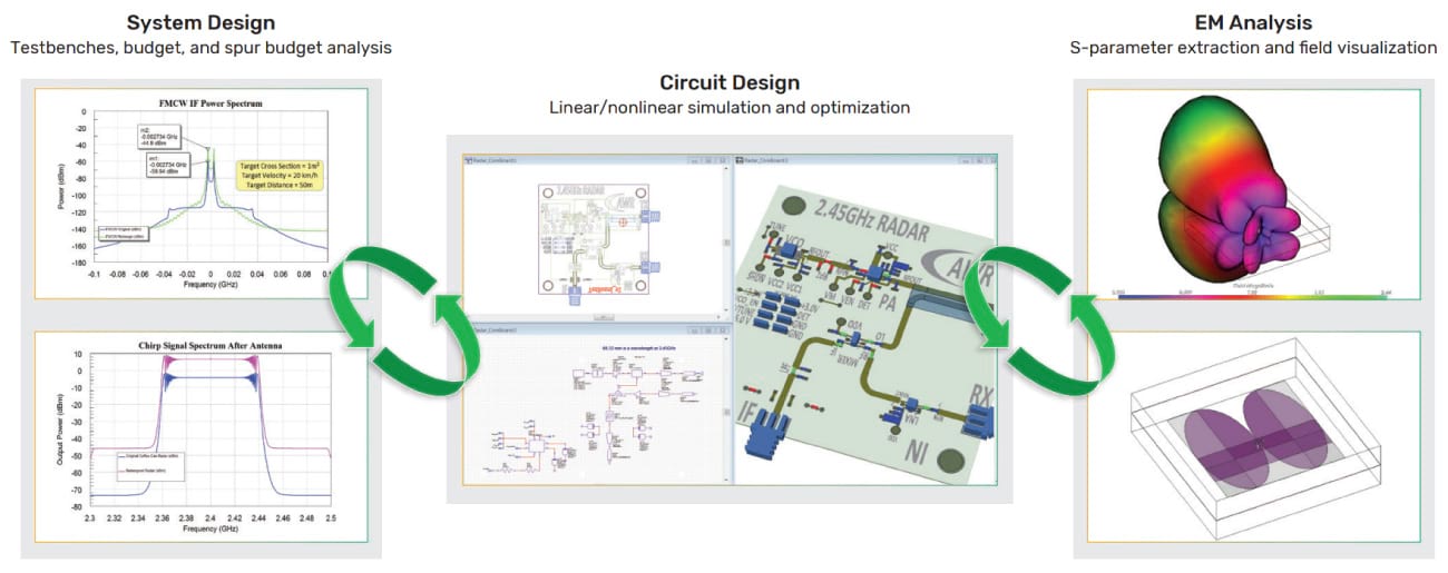
spectrum. In addition, since these products are developed by diverse engineering teams across multiple design tools, RF design software must provide interoperability with the broader class of EDA used in the development of mixed-signal electronic systems. To optimize product development throughput and successful designs, this software must offer automation that supports engineering productivity alongside seamlessly integrated circuit, system, and electromagnetic (EM) simulation, synthesis, and optimization. These capabilities are built into Cadence AWR Design Environment software, inclusive of AWR Microwave Office, AWR Visual System Simulator(VSS), AWR AXIEM, and AWR Analyst software, providing a robust and complete platform for RF/microwave engineers to develop next-generation communication and radar front-end electronics.
Furthermore, with the Version 15 (V15) release of its AWR Design Environment software, Cadence is addressing RF/ microwave design and integration through the company’s Intelligent System Design strategy, which delivers computational software capabilities across all design elements of electronic systems. At the core of this strategy is design excellence, including an optimized EDA portfolio of tools with best-in-class RF, microwave, and mmWave circuit, system, and EM analysis, IP for semiconductor, package, and PCB design, and scalable access in the cloud.
The V15 Advantage
AWR Design Environment V15 offers key new and improved technologies that provide greater design efficiency and first-pass success to engineering teams developing and integrating III-V and silicon (Si) integrated circuits (ICs), multi-technology modules, and PCB assemblies. Engineering productivity is improved with new analyses, faster and higher capacity simulation technologies, time-saving design automation, and 5G New Radio (NR)-compliant testbenches that support power amplifier (PA) and antenna/array design, EM modeling, and RF/ microwave integration across heterogenous technologies.
Design Environment and Automation
New design environment and automation features help individual engineers and engineering teams be more efficient in their design entry, data display, and project management. Designers can adjust optimization goals directly from response plots, route design rule-compliant intelligent nets (iNets) in real-time, import Gerber-based layout designs into AWR Design Environment for EM analysis, and provide more user capabilities for the design task at hand.
| AWR Design Environment V15 Highlights | ||||
|---|---|---|---|---|
| Environment/ Automation | Circuit Simulation | EM Simulation | System Simulation | Physical Design/ Layout |
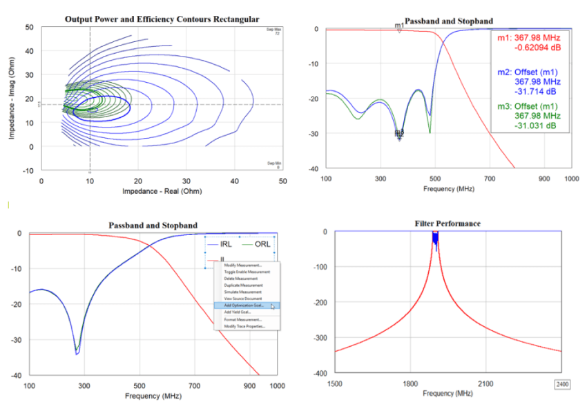
Load-pull contours on rectangular plots Template-based measurements Add/edit optimization goals directly on graphs Edit axes directly on plots Color-coded markers Equation grouping |
Fast, rigorous stability analysis Low-frequency loadpull for two-tone excitations Integrated TX-Line calculator/synthesis Network synthesis with PDK/vendor components |
Faster, more robust adaptive meshing Fast, accurate DC solver Peak antenna measurements |
Preconfigured 5G NR testbenches libraries Phased array MIMO bus support PA linearization with digital predistortion (DPD) |
Real-time DRC compliant iNets routing guides Mixed physical units/ grid support Two-click data entry mode Resize layout objects with property page editing Gerber file import for EM analysis |
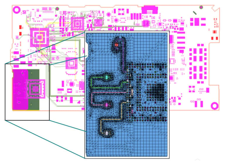
Addressing the increasing size and complexity of RF/ mixed-signal electronic systems, the new, faster layout and 3D viewer rendering capability in V15 enables users to zoom in and out and rotate large structures to inspect the physical design from any and all angles without any lag time. Large boards imported as IPC-2581 or ODB++ files from Cadence Allegro® PCB Designer or other layout tools can be readily inspected visually before editing and preparation for EM analysis using the PCB editing wizard.
In addition, V15 of AWR software expands support for RF/ microwave front-end component integration within multi-technology systems. The layer process definition file (LPF) in AWR Microwave Office defines the processing layers and parameters for the physical layout design. For analysis of heterogeneous substrates and multi-chip modules utilizing different semiconductor processes and laminates, AWR Design Environment software supports multiple process definitions within a single hierarchical project. The software’s “per-process technology” native LPF units, allow different processes to specify units that are most appropriate for a given technology (e.g., mils or microns).
PA Simulation and Design Support
To meet bandwidth requirements, 5G systems aggregate contiguous and discontiguous spectrum at sub-6GHz and take advantage of the available bandwidth at mmWave frequencies, both of which put pressure on PA designers who need to address linearity and efficiency concerns in the presence of high peak-to-average power ratios (PAPRs).
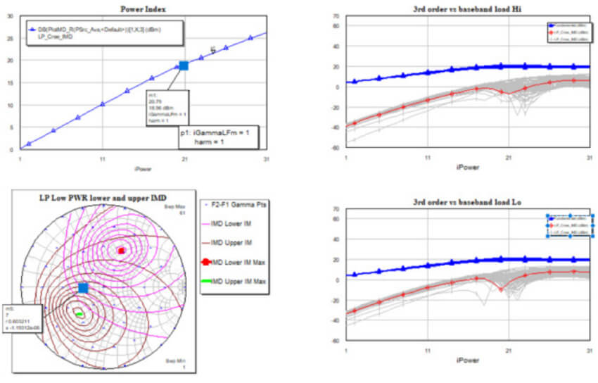
In wideband PAs, baseband impedance variations over bandwidth can impact device linearity, resulting in intermodulation distortion (IMD) levels that vary asymmetrically with instantaneous signal bandwidth. This issue, which is associated with memory effects, is commonly addressed by using video bypass capacitors to terminate the baseband impedance with short circuits.
However, performance can be improved by considering alternative baseband impedance conditions. For instance, PA developers have shown significant improvements in linearity when active, baseband injection architectures such as envelope tracking (ET) are employed.
V15 of AWR software allows designers to optimize PA linearity performance through video band load-pull analysis of PAs operating under two-tone excitations. Designers can plot IMD and third-order intercept point (IP3) results as a function of (F2-F1) impedance, directly investigating intermodulation products over swept input power.
Load-pull analysis also supports impedance tuning at the 4th and 5th harmonics as well as the ability to generate contours on rectangular plots for enhanced visualization of performance versus load impedance.
Transistors designed for mmWave amplifier designs have high gain at lower frequencies, making them more prone to potential spurious oscillations. Stability analysis is critical to amplifier design and optimization, especially for these high-gain devices.
The commonly used K- and μ-factors, derived from linear circuit simulation, can accurately predict whether a 2-port network is unconditionally stable, yet they cannot detect instabilities for multi-stage amplifiers or devices connected in parallel. Other stability analyses such as NDF and loop gain techniques, can overcome these limitations but do so at the cost of extensive computations, making them too slow for performing optimization.
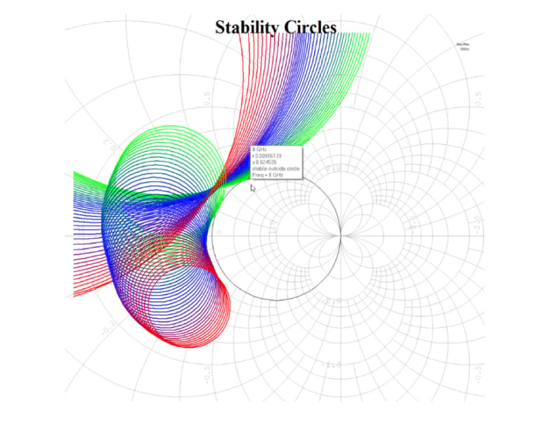
The loop gain envelope technique for evaluating the envelope of traditional loop gain stability circles has been shown to cut the simulation time of this more rigorous approach to stability analysis from hours down to seconds, making it ideal for stability optimization. V15 of AWR software supports this method with a loop gain envelope code module and equation block that can be easily applied to new amplifier designs. The support for loop gain envelope stability analysis offers designers the following benefits:
The loop gain envelope technique for evaluating the envelope of traditional loop gain stability circles has been shown to cut the simulation time of this more rigorous approach to stability analysis from hours down to seconds, making it ideal for stability optimization. V15 of AWR software supports this method with a loop gain envelope code module and equation block that can be easily applied to new amplifier designs. The support for loop gain envelope stability analysis offers designers the following benefits:
-
 The stability and margin of stability of each device within an amplifier is quantified.
 - The input and output terminations are analytically applied, increasing analysis speed.
- Fewer N phase combination evaluations are required, increasing analysis speed.
- Due to the speed enhancements, optimization of phase margin for each device within an amplifier is now possible.
Synthesis Accelerates RF Designs
The characteristic impedance and electrical length (delay) of transmission lines represent two important design parameters used to control the frequency-dependent circuit response of passive RF/microwave circuits such as quarter-wave impedance transformers, Wilkinson power dividers/combiners, hybrid couplers, filters, and more.
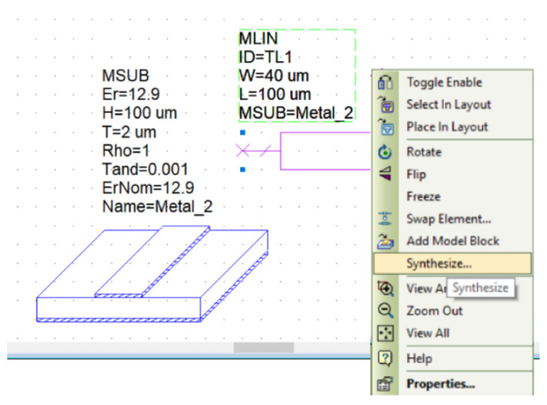
Using AWR Design Environment V15, designers can directly synthesize the physical attributes (width, length) of these microstrip, stripline, or coplanar waveguide structures for a given substrate based on the desired electrical characteristics.
Likewise, the electrical characteristics can be calculated directly from the physical properties of the single or edge-coupled transmission line placed in the schematic. Synthesis of circuit model parameters provides vital data for generating accurate layout of these transmission lines without having to invoke the transmission line calculator and manually transfer the results into the transmission line property dialog box.
Further expanding synthesis as a powerful design aid, the enhanced network synthesis wizard, expedites impedance-matching network development for challenging wideand multi-band PA and inter-stage impedance-matching circuits by allowing users to generate optimum matching networks directly using components from the AWR Microwave Office vendor library for surface-mount PCB-based designs. This capability also supports models from process design kits (PDKs), thereby extending the matching circuit synthesis feature to include monolithic microwave integrated circuit (MMIC) PAs and other MMIC-based designs.
EM Simulation and Antennas
To enhance the speed and capacity of EM analysis for IC, package and board structures, AWR AXIEM meshing and solver technologies have undergone several key improvements, resulting in improved mesh quality for faster simulation run times and the ability to solve larger problems with a reduced mesh.
AWR Design Environment V15 can now detect and remove problematic mesh facets automatically with robust healing of high aspect ratio facets (HARF). The software supports subnanometer (nm) z-axis resolution of metals and dielectrics (previously rounded to the nearest nm), to provide faster modeling of sub-nm multi-layer IC structures such as metal-insulator-metal (MIM) capacitors.
Both large PCBs and silicon (Si) on-chip components can contain manufacturing features that do not impact RF performance but can slow down EM analysis by increasing the problem size. In AWR Design Environment V15, shape pre-processing rules have been expanded to better address Si processes (handle large number of metal layers) and merge via arrays on user-specified layers and inside/ outside a specified region.
In addition, enhancements to the AWR AXIEM DC solver (used for characterizing low-frequency behavior, such as bias networks) employ new sparse symmetric matrix technology, resulting in a 10- to 100-fold savings in time and memory usage.
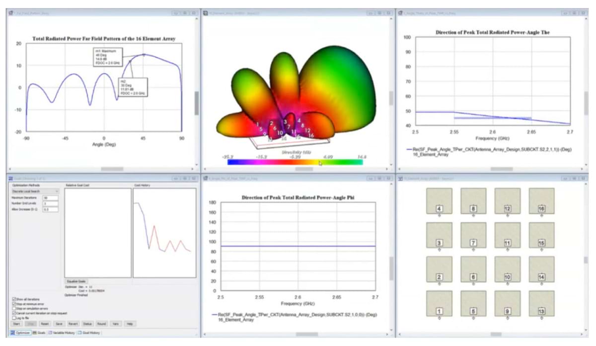
AWR Design Environment software allows users to look at various antenna performance metrics such as total power, or the power in a particular polarization across some "cut" of the antenna. V15 of the software introduces a new class of peak antenna measurements, which enables designers to easily set up optimization goals and variables to direct the performance of the antenna.
For example, an antenna designer can easily change an AWR AXIEM or Analyst software-based phased array design from pointing boresight to some specified theta. In addition, users can now plot antenna radiation pattern peaks for E-Phi, E-Theta, E-LHCP, E-RHCP, and total radiate power as a function of swept frequency directly from measurement and optimization dialog boxes. Both static- and circuitdriven variations of these measurements are available.
Antenna designers can now directly simulate antenna loading, matching networks, and model frequencydependent circuit components within an Analyst model. Resistor, inductor, capacitor (RLC) components and matching networks that are embedded in the antenna can be simulated without the need for additional ports and use of circuit co-simulation. Model frequency-dependent components in the antenna simulation can also be used to design reconfigurable or more broadband antennas.
5G NR Library and DPD Models
The 5G NR library offers easy-to-configure signal sources and receivers that can be used to evaluate RF components and/or RF links using system-level measurements. New testbenches accelerate the component design and evaluation process with preconfigured 5G NR TX and RX blocks and measurements supporting TX/RX functionality for both downlink and uplink.
Flexible signal configurations support variable signal power, carrier frequency, modulation and coding scheme (MCS), bandwidth and subcarrier spacing to meet the requirements defined in the specifications for sub-6GHz (FR1) as well as mmWave (FR2) bands.
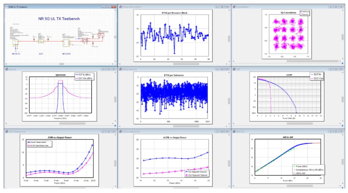
The 5G NR receiver testbenches include preconfigured sensitivity measurements such as bit error rate (BER), block error rate (BLER), and throughput. The new 5G NR TX testbenches support transmitter simulations and device validation with various preconfigured measurements to analyze performance metrics such as complementary cumulative distribution function (CCDF), AM to AM/PM, spectrum, error-vector magnitude (EVM), adjacent channel power ratio (ACPR), IQ constellation, and more.
Downlink test models, defined for both sub-6GHz band (FR1) and mmWave band (FR2), provide 5G NR signals for performing measurements, such as basestation output power, unwanted emissions, spurious emissions, intermodulations, EVM for various modulation types such as quadrature phase-shift keying (QPSK), and 16, 64, and 256 quadrature amplitude modulation (QAM), and frequency error. The example projects, which are available through the AWR KnowledgeBase, demonstrate NR 5G transmitters and receivers configured according to Third Generation Partnership Project (3GPP) TS 38.141 Section 4.9.2 and include the preconfigured system diagrams and relevant result graphs, ready for simulation.
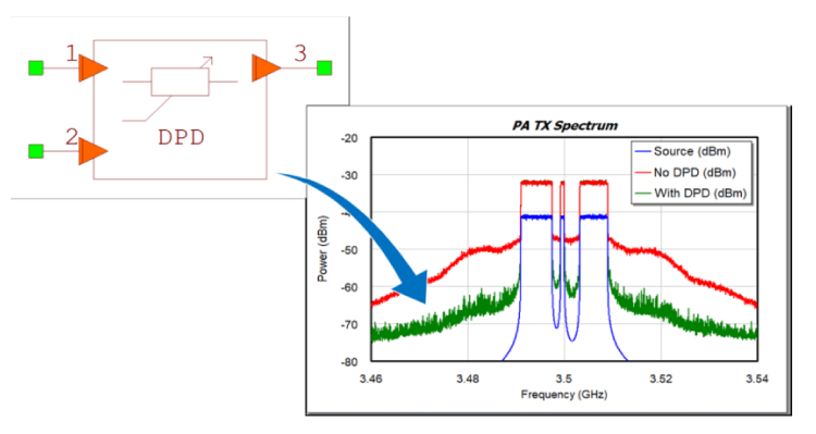
AWR Design Environment V15 also includes a new digital predistortion (DPD) block providing algorithms to linearize nonlinear amplifiers. This DPD model supports memory polynomial, generalized memory polynomial, dynamic deviation reduction of second order (DDR2), and lookup tables. To demonstrate the new model, an example project has been created (available from the AWR KnowledgeBase) using a driver amp feeding a PA implemented in AWR Microwave Office software. The AWR Microwave Office subcircuit is excited in AWR VSS system design software by an orthogonal frequency-division multiplexing (OFDM) signal at 3.5GHz configured to simulate multi-user-type operation.
The DPD model uses a feedback signal from the device output which, along with the source signal, is used for initial calculations of the selected algorithm and then for incremental updates. The block offers various solvers that can be used for the initial DPD setup. Results compare device performance with and without the DPD, showing improvements in spectral regrowth, IQ constellation distortion, and CCDF. Options for commercial DPD solutions are also available, allowing users to run the same algorithms in simulations as in the lab.
Summary
AWR Design Environment V15 software brings new and enhanced RF/microwave design and simulation to the Cadence portfolio of EDA solutions. Advanced design automation optimizes engineering throughput and productivity by reducing manual design tasks and supporting tool interoperability.
New circuit simulation capabilities address fast and rigorous nonlinear stability analysis for multi-stage and balanced amplifiers, and video-band load pull to optimize low-frequency impedance terminations for reduced intermodulation distortion. Network synthesis supports impedance network development using vendor components and PDKs, and a new integrated transmission-line calculator and synthesis capabilities launched directly from schematic.
Robust simulation engines solve large structures more quickly using EM analysis with enhanced meshing and smart geometry handling for chip, package, and board characterization. Preconfigured, 5G NR-compliant testbenches provide signal sources and measurements for PA and RF link validation.