Webinar
Cadence-Based RF-Design Flow for X-FAB 130nm RF-SOI Technology

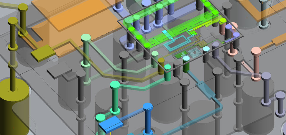
With the increasing complexity of RF circuits and all electronic devices in general, it has become necessary for design engineers to predict the behavior of these systems with simulation tools using accurate models to ensure “first-time-right” success. Ousmane Sow of X-Fab shares how the company provides customers a complete circuit design flow including electrical simulation, layout, physical verifications, parasitic extraction, and electromagnetic (EM) simulation. This presentation focuses on a complete Cadence-based design flow developed for X-FAB’s 130nm RF-SOI technology. After a short presentation of the RF-SOI technology, we explore the Cadence EMX stack-up and its validation using inductor test cases. Then, the complete RF flow is exercised on a 6GHz low-noise amplifier (LNA) compliant with the IEEE Wi-Fi 802.11ac standard. Next, we perform a hardware model correlation showing a good fit. This result validates the flow. The LNA design is available at myxfab.com as a reference kit.