Datasheet
RF PCB Design with AWR Software
Simulation and design flow technologies for high-frequency PCB development
Demand for increased functionality is driving more complex structures in modern highfrequency PCBs designed for a range of specialized radar and communication applications. Cadence AWR Design Environment software supports accurate modeling of PCB transmission media from the RF-signal path to digital control and DC-bias lines. Circuit/ system and electromagnetic (EM) co-simulation provides first-pass design success with complete PCB analysis of surface-mount components, interconnecting transmission lines, and embedded and distributed passive elements, as well as EM verification. Design automation supports a flexible workflow that operates as a standalone solution or part of an enterprise-level PCB system.
Overview
RF PCB Design Advantage
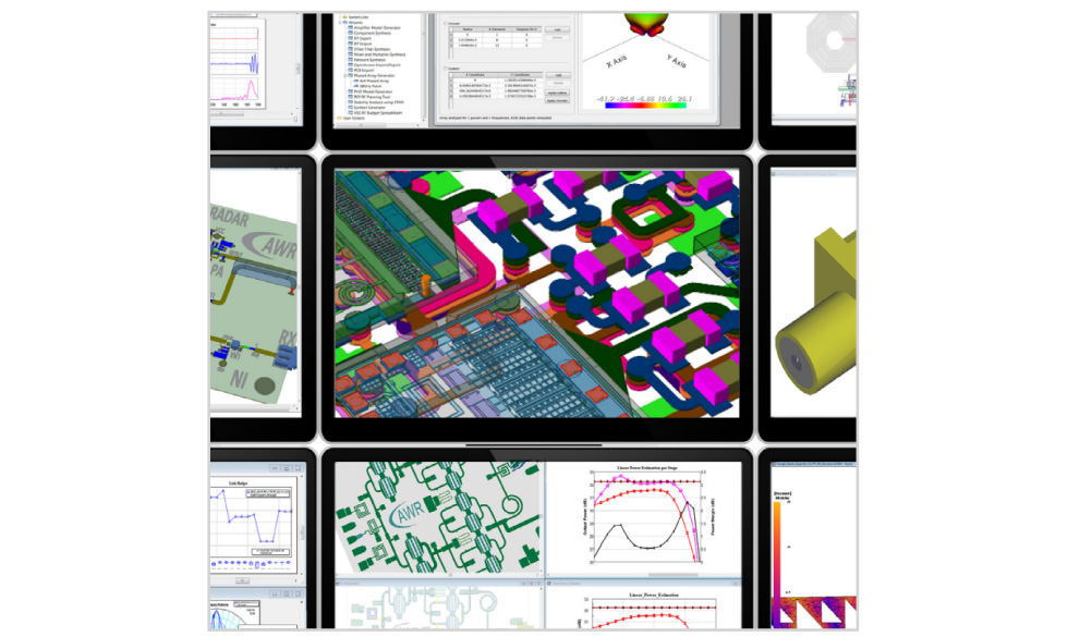
Layout-driven schematic elements within the AWR Design Environment platform enable designers to adaptively model the RF signal path and create an electrical/physical design with RF-aware elements ready for accurate simulation.
Cadence AWR Microwave Office circuit simulation software provides designers with rapid design entry/ editing that automatically resizes junction and discontinuity models as circuits are tuned, optimized, or re-routed, all without changing the schematic. Integrated EM simulation technology supports a wide range of PCB modeling needs and design flows.
Product Strengths
Design Flow Automation
AWR software provides PCB compatibility with a host of file formats, enabling designers to readily access the best tools for the task at hand. Starting from PCB physical design in layout form, standard PCB formats such as DXF, Gerber, ODB++, and IPC-2581 are supported, which provides plug-and-play compatibility with layout tools from third-party vendors. The PCB import wizard offers advanced layout selection/editing in preparation for more efficient EM analysis.
In addition, the proprietary iNet intelligent net technology automates layout implementation of interconnects as wires on a schematic. A layout net, represented as a “rat’s nest,” is selected in the layout and then routed simply by clicking the path from component to component, after which the line is routed using specified default vertical and horizontal routing layers and widths.
EM Analysis
The Cadence AWR AXIEM 3D proprietary full-wave planar EM simulator uses method-of-moments (MoM) fast-solver technology to readily analyze distributed PCB components, transmission lines, and layer-to-layer PCB interconnects such as vias. Designers can extract S-parameters directly within their PCB design and visualize fields/currents to identify parasitic coupling and resonances.
The automated circuit extraction (ACE) interconnect analysis tool converts complex PCBs into high-frequency circuit netlists, including every crossover, via, and multilayer coupled-line model. ACE technology uses MoM and FEM solvers on the densest parts of any design to improve accuracy by focusing less on lines that have little impact on circuit behavior. The ACE coupling radius discriminator isolates couplings that limit board performance.
Tool Interoperability
Cadence AWR Connected third-party software/hardware solutions link AWR software within a broader PCB subsystem design flow, including enterprise-level layout tools, alternative EM/thermal simulators, and design-rule check (DRC)/layout vs. schematic (LVS) technologies.
Features
Highlights
-
 Powerful design entry/automation and comprehensive vendor libraries
 - Accurate, fast, and robust harmonic balance (HB) simulation
- AWR AXIEM analysis for automated layout editing, design verification, and parasitic extraction
- Cadence AWR Analyst 3D FEM EM analysis for modeling 3D structures
- EM Socket for integration with third-party EM tools
- ACE technology for interconnect modeling