Content Type
AWR Analyst
Full 3D finite element method EM analysis software
Cadence AWR Analyst arbitrary 3D finite element method (FEM) electromagnetic (EM) simulation and analysis software within the Cadence AWR Design Environment platform accelerates high-frequency product development from early physical design characterization through to full 3D EM verification. The 3D FEM solver provides fast and accurate EM analysis so engineers can achieve higher performance in less development time for greater first-pass success.
Overview
AWR Software Platform
With the AWR Analyst software, you can detect and diagnose design problems that can cause products to fail performance requirements. A 3DEM simulation fully integrated and readily available within an RF/microwave component design flow enables designers to identify and eliminate potential failures.
Access and create libraries of parameterized EM cells (PCells) for common and custom 3D interconnects and passive PCB and IC components that enable reuse. Incorporation of complex structures with a simple drag and place captures true electrical responses throughout the design process.
In addition, you can accurately and rapidly characterize interconnect structures, dense circuitry, and antenna structures of all sizes with full 3D FEM solver technology with adaptive volumetric tetrahedral meshing, direct and iterative solvers, and discrete and fast-frequency sweeps.
Product Strengths
Design Exploration
Automatically improve performance and mitigate design problems from unforeseen resonances and coupling between structures with 3D EM parametric studies that support optimization, tuning, and yield analysis. Combine spectral decomposition with remote computing to expedite simulation run times and provide answers faster.
3D Modeling
Readily characterize passive 3D components, distributed planar structures, interconnects such as vias and bondwires, complex electronic packaging, and waveguide structures directly within a circuit network. Support for 3D CAD file formats like IGES, STEP, and STL allows designers to perform EM analysis on structures from alternative CAD tools.
Optimization and Yield
Perform accurate design diagnostics such as yield analysis and optimization for passive components and complex interconnects, capturing true coupling and parasitic effects of circuit topologies that are specified parametrically and/or defined through rules-based shape modifiers/de-featuring.
Visualization
Plot color-coded currents and electric field strength directly on an analyzed structure to gain insight into component behavior and the source of potential design failure.
We chose AWR software because of the proven success of AntSyn and Analyst. The resulting designs worked from the very start and removed the iteration and experimentation usually required in antenna design efforts.
Mark Ross, Striiv
Simulation Technologies
Adaptive Meshing
3D adaptive meshing algorithms use a highly robust volumetric tetrahedron meshing technique to automatically provide accurate results with minimal set-up effort or manual intervention. If necessary, user control of the mesh can be enabled for individual shapes using the 3D editor.
Finite Element Analysis
The proprietary and state-of-the-art full-wave FEM EM analysis technology within Analyst software supports direct and iterative solvers, as well as discrete and fast-frequency sweeps. Developed over many decades, the technology has been optimized for scalability and accuracy.
Antenna Analysis
Analyze 3D and 2D antennas, including patch antennas and antenna arrays on finite dielectrics, plot near- and far-field radiation patterns and simulate key antenna metrics such as gain, directivity, efficiency, side lobes, return loss, surface currents, and more
Features
Highlights
-
 Layout/Drawing Editor – 2D/3D construction and views
 - Proprietary FEM full-wave technology
- Meshing Technology – Automatic and adaptive meshing
- Numerous sources and excitations for ports
- Visualization and results post - processing
- Parametric Studies – Optimization, tuning, and yield analysis
- HPC – Multi-core configurations and asynchronous simulation
Applications and Technologies
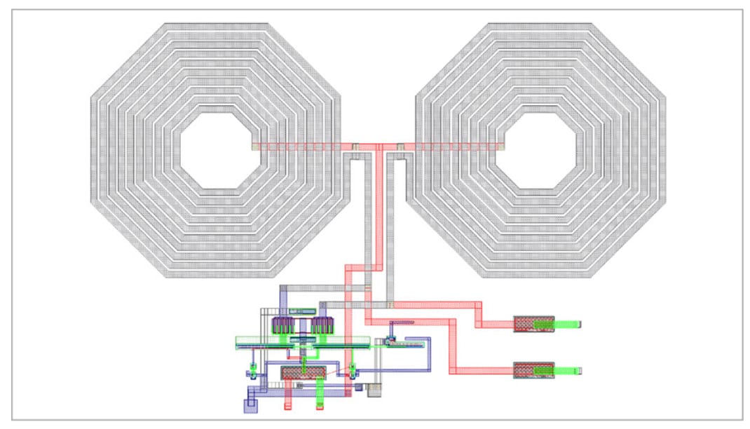
On-Chip Passive
Successful passive component design focuses on reducing the footprint, costs, and associated insertion losses, while providing increased power-handling capabilities. Capture the broadband performance of IC layout and on-chip passives by accurately simulating the electrical behavior resulting from die-level vias, tapered lines, spiral inductors, and other passive semiconductor structures. Define Analyst EM structures from extruded 2D shapes and vias as conductors or dielectrics. Passive component performance such as frequency-dependent impedance/reactance or quality factor (Q factor) can be determined.
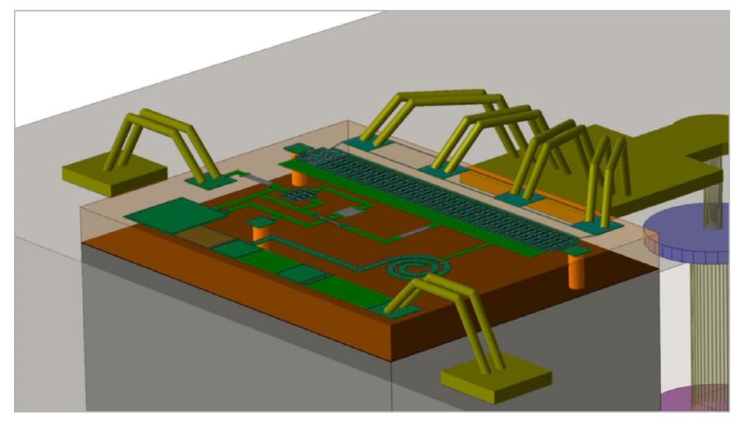
IC, PCB, and Packaging
The advanced solver technology provides fast and accurate analysis of the 3D structures/interconnects within today’s complex high-frequency electronics. Simulate advanced package and board interconnects, including air bridges, bondwires, bumps, and solder balls between the die and its package or the package and its board with 3DEM accuracy, improving end-product performance. Analyst software can simulate the response of finite (area) dielectric structures and should be used over a planar EM solver when the RF behavior of metal interconnects and distributed components may be impacted by proximity to the edge of a substrate.
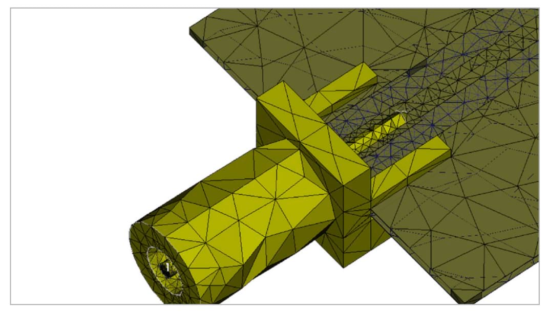
Antennas and Connectors
Arbitrary 3D structures such as horn and helix antennas can be modeled to extract S-parameters for voltage standing-wave ratio (VSWR), return loss, and radiation patterns. A variety of pre-designed common RF/microwave parts such as connectors and antennas are included and, in addition, users can create custom PCells as needed with the Analyst 3D editor. Simulation and modeling capabilities support additional custom 3D constructs, such as bondwires, ball grid arrays, tapered vias, and more. New peak antenna measurements support performance metrics such as total radiated power, or power in a particular polarization across the “cut” of a radiation pattern as a function of swept frequency or other user-defined swept parameters.